Image sensor and image sensor forming method

An image sensor and semiconductor technology, applied in semiconductor/solid-state device manufacturing, electrical components, circuits, etc., can solve the problems of deviation between positions, affecting the uniformity of image sensors, affecting the performance of image sensors, etc., to improve uniformity, Thickness is easy to accurately control and the effect of improving performance

Inactive Publication Date: 2016-06-01
SEMICON MFG INT (SHANGHAI) CORP
View PDF4 Cites 3 Cited by
  • Summary
  • Abstract
  • Description
  • Claims
  • Application Information

AI Technical Summary

Problems solved by technology

However, due to the deviation of the photolithography process, there is a deviation between the positions of the P-type pinning layers of different pixels, which affects the uniformity of the performance of different pixel units of the image sensor, thereby affecting the performance of the image sensor

Method used


Image

  • Image sensor and image sensor forming method
  • Image sensor and image sensor forming method
  • Image sensor and image sensor forming method

Examples


Embodiment Construction

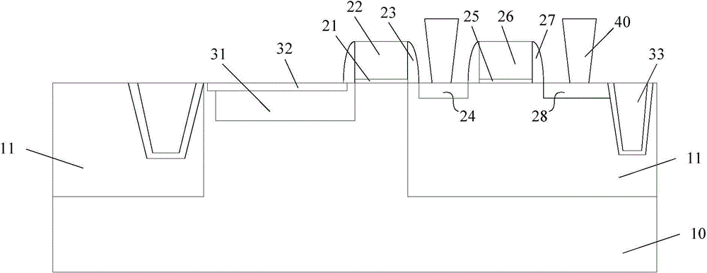
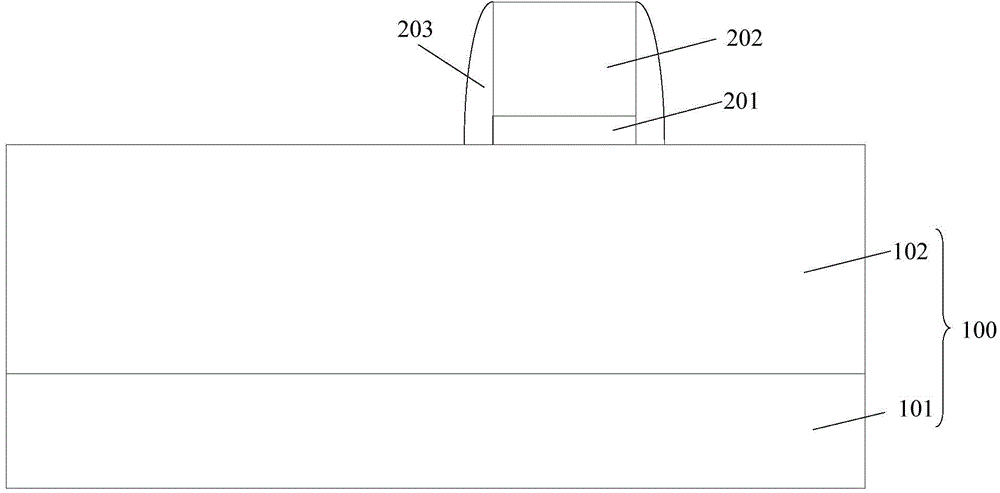
[0034]As mentioned in the background art, the performance of the image sensor formed in the prior art needs to be further improved. There is a part of the N-type doped region between the P-type pinning layer and the channel region of the transfer transistor, and the distance between the P-type pinning layer and the first gate structure is too small, which will cause the P-type pinning layer and the transfer transistor Part of the N-type doped region between the channel regions is pinched off, which affects the transmission of photoelectrons, and the dopant ions in the P-type pinning layer diffuse to the channel region, affecting the transmission of the channel region of the transistor. width. Due to the size of the patterned photoresist layer formed by photolithography, there will be deviations in different pixel units, resulting in different distances between the P-type pinning layer and the first gate structure of different pixel units, so that the N-type doping The channel...


PUM


Abstract

The invention provides an image sensor and an image sensor forming method. The image sensor forming method comprises the steps of providing a semiconductor substrate; forming a gate structure which covers partially semiconductor substrate on the semiconductor substrate; forming an N-type doped region in the semiconductor substrate at one side of the gate structure; forming a sacrificial layer on the surface of the sidewall of the gate structure, wherein the sacrificial layer at one side of the gate structure covers partial N-type doped region; forming a P-type pinning layer on the surface, which is not covered by the sacrificial layer, of the N-type doped region; and removing the sacrificial layer for exposing partial N-type doped region which is not covered by the P-type pinning layer. The image sensor forming method can improve performance of the image sensor.

Description

technical field [0001] The invention relates to the technical field of semiconductors, in particular to an image sensor and a forming method thereof. Background technique [0002] Image sensors are semiconductor devices that convert optical image signals into electrical signals. Products with image sensors as key components have become the focus of the current and future industry, attracting investment from many manufacturers. Divided by product category, image sensor products are mainly divided into Charge-coupled Device image sensor (CCD image sensor for short), Complementary Metal Oxide Semiconductor image sensor (Complementary Metal Oxide Semiconductor image sensor, CMOS sensor for short). CMOS image sensor is a fast-growing solid-state image sensor. Since the image sensor part and the control circuit part of the CMOS image sensor are integrated in the same chip, the CMOS image sensor has small size, low power consumption, and low price. Compared with The traditional C...

Claims


Application Information

Patent Timeline
Patent Type & Authority Applications(China)
IPC IPC(8): H01L27/146H01L21/8238
Inventor 倪景华李凤莲
Owner SEMICON MFG INT (SHANGHAI) CORP
Why Eureka
Try Eureka