Electrical field assisted writing magnetic tunnel junction unit and writing method thereof
A magnetic tunnel junction, electric field assisted technology, applied in the field of micro-nano electronics, can solve the problems of electric field assisted writing constraints, the inability to control the magnitude of the electric field effect at the I/FL interface, etc., to enhance the electric field modulation effect and avoid the aging of the barrier layer. , the effect of reducing the difficulty of writing
- Summary
- Abstract
- Description
- Claims
- Application Information
AI Technical Summary
Problems solved by technology
Method used
Image
Examples
Embodiment 1
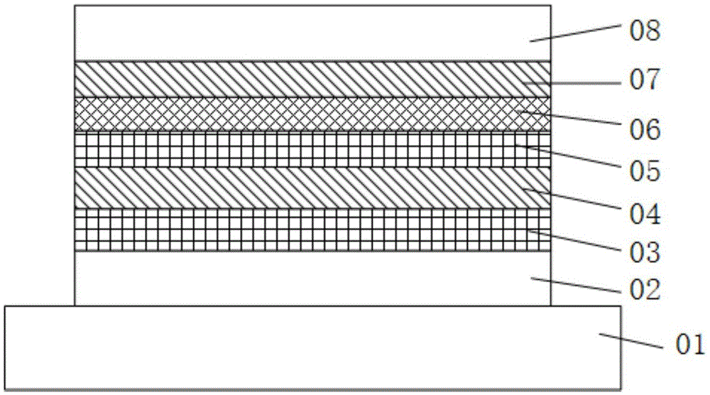
[0043] combine figure 1 , the structure of the above-mentioned magnetic tunnel junction includes: the first electrode layer Cu on the substrate, and the first magnetic layer CoFeB, the first insulating tunneling layer MgO, the second magnetic layer CoFeB, the A metal layer Pt, a second insulating layer MgO and a second electrode layer Cu.
[0044] Wherein, the thickness of the first metal layer Pt is 0.5nm, and the electric field / voltage generated by the write pulse can greatly reduce the magnetic anisotropy of the second magnetic layer, thereby reducing the write power consumption. The substrate is a thermally oxidized Si sheet or a CMOS chip
Embodiment 2
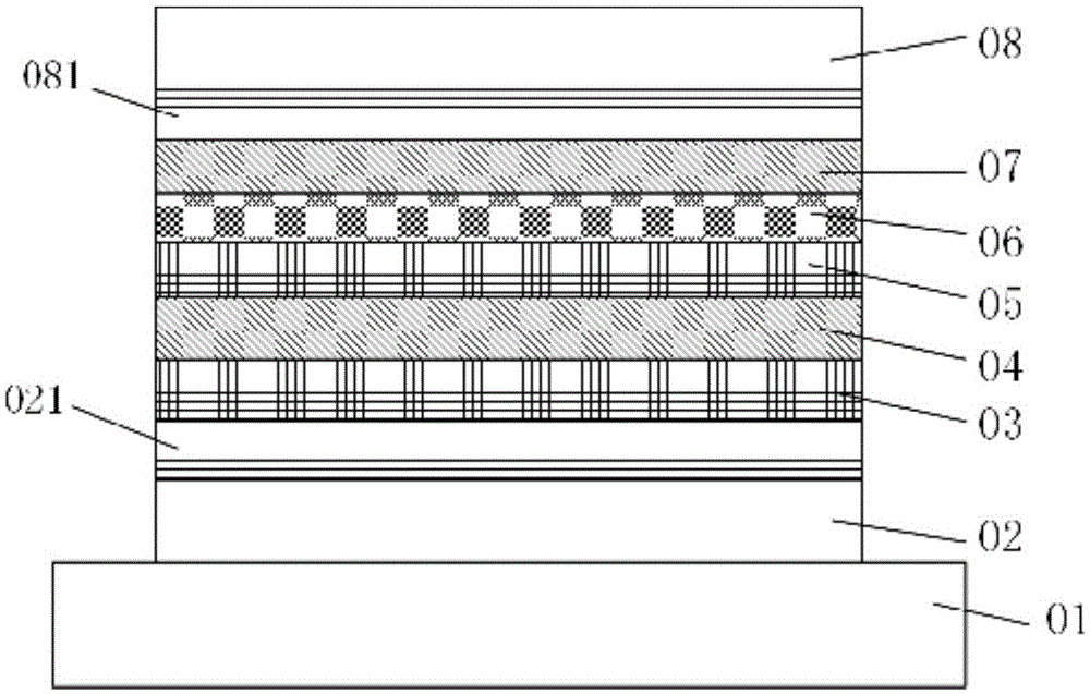
[0046] combine figure 2 , the structure of the magnetic tunnel junction includes: the first electrode layer Cu on the substrate, and the seed layer Ta formed on the first electrode layer in sequence, the first magnetic layer CoFeB, the first insulating tunneling layer MgO, the second magnetic layer CoFeB, the first metal layer Pt, the second insulating layer MgO, the covering layer Ta and the second electrode layer Cu.
[0047] Wherein, the thickness of the first metal layer Pt is 0.5nm, and the substrate is a thermally oxidized Si sheet or a CMOS chip.
Embodiment 3
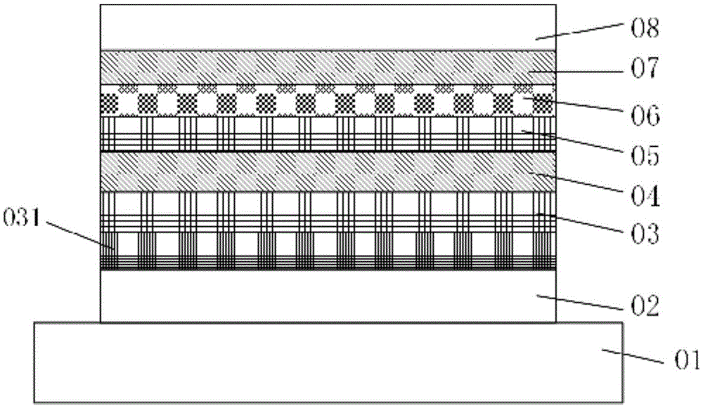
[0049] combine image 3 , the structure of the above-mentioned magnetic tunnel junction includes: the first electrode layer Cu on the substrate, and the seed layer Ta formed on the first electrode layer in turn, the third magnetic layer (Co / Pt) n (The subscript n represents a multilayer film structure), the first magnetic layer CoFeB, the first insulating tunneling layer MgO, the second magnetic layer CoFeB, the first metal layer Pt, the second insulating layer MgO, and the second electrode layer Cu .
[0050] Wherein, the thickness of the first metal layer Pt is 0.5nm; the third magnetic layer has high vertical anisotropy and is ferromagnetically coupled with the first magnetic layer; the substrate is a thermally oxidized Si sheet or a CMOS chip.
PUM
| Property | Measurement | Unit |
|---|---|---|
| Thickness | aaaaa | aaaaa |
| Thickness | aaaaa | aaaaa |
| Thickness | aaaaa | aaaaa |
Abstract
Description
Claims
Application Information


