Double-layer sectioned SOI LIGBT device and manufacturing method thereof

A device and double-layer technology, applied in the field of electronics, can solve the problems of lowering the breakdown voltage, poor thermal conductivity of the oxide layer, self-heating effect, etc., and achieve the effect of increasing the breakdown voltage and reducing the self-heating effect

Active Publication Date: 2016-06-01
NANJING UNIV OF POSTS & TELECOMM
View PDF4 Cites 6 Cited by
  • Summary
  • Abstract
  • Description
  • Claims
  • Application Information

AI Technical Summary

Problems solved by technology

The difference from LDMOS is that LIGBT is a bipolar device. When it is turned on, there is not only electron current, but the anode P+ will inject holes into the drift region to generate electron current. In the absence of an isolation layer, some holes will continue to flow to the substrate. injection, causing considerable leakage current
Therefore, there are two substrate isolation methods, one is the reverse PN junction plus a current-conducting structure. The disadvantage of this structure is that it requires heavy doping, which greatly reduces the breakdown voltage.
One is SOI isolation. In this way, the oxide layer is used to directly isolate the substrate and the drift region, which can effectively reduce the leakage current, but because only the drift region is under pressure, the breakdown voltage is also reduced. At the same time, because of the heat conduction of the oxide layer Poor capacity, can cause self-heating effect

Method used


Image

  • Double-layer sectioned SOI LIGBT device and manufacturing method thereof
  • Double-layer sectioned SOI LIGBT device and manufacturing method thereof
  • Double-layer sectioned SOI LIGBT device and manufacturing method thereof

Examples


Embodiment Construction

[0024] Below in conjunction with accompanying drawing, technical scheme of the present invention is described in further detail:

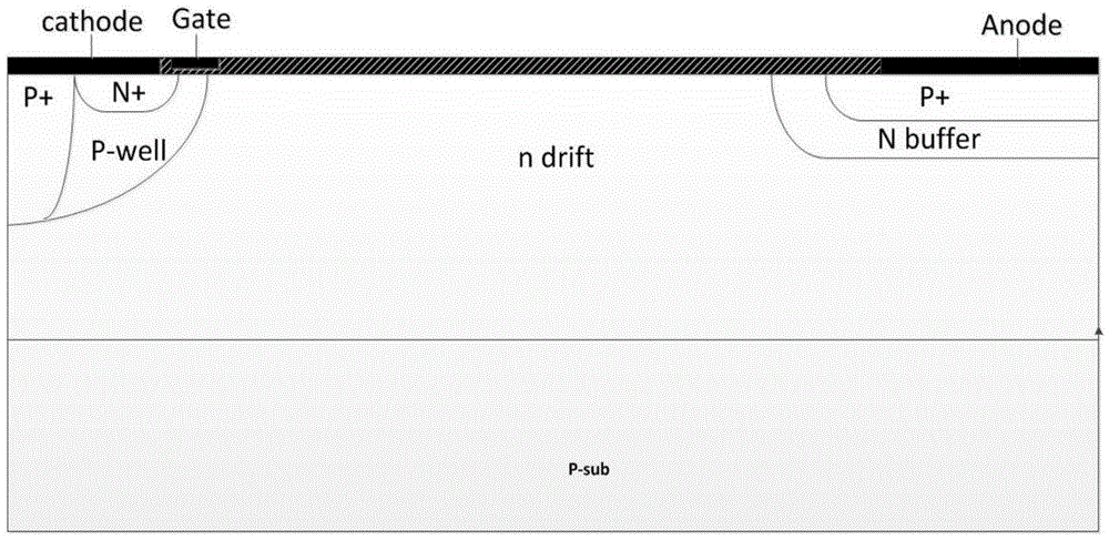
[0025] like figure 1 As shown, the common LIGBT device structure does not have an isolation structure between the working area and the substrate to deal with the leakage current of the substrate, so a large number of holes are directly injected into the substrate in the working state, which seriously affects the device performance.

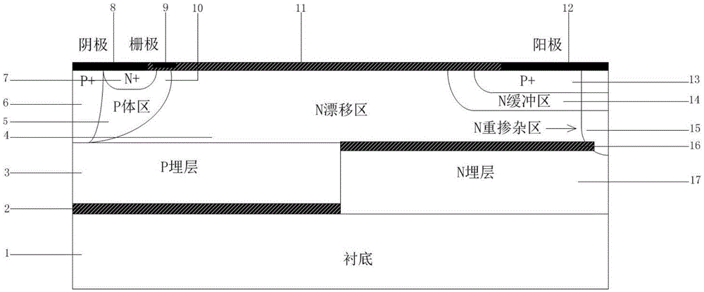
[0026] like image 3 As shown, a double-layer partial SOIL IGBT device includes a silicon substrate 1, on which a first buried oxide layer 2 and an N buried layer 17 are sequentially arranged from left to right, and the upper surface of the N buried layer 17 is higher than the first The upper surface of a buried oxide layer 2, the first buried oxide layer is provided with a P buried layer 3, the N buried layer 17 is provided with a second buried oxide layer 16, the upper surface of the P buried layer 3 and the second ...


PUM


Abstract

The invention discloses a double-layer sectioned SOI LIGBT device. The double-layer sectioned SOI LIGBT device comprises a silicon substrate; a first buried oxide layer and an N buried layer are sequentially arranged on the silicon substrate from left to right; the upper surface of the N buried layer is higher than the upper surface of the first buried oxide layer; a P buried layer is arranged on the first buried oxide layer; a second buried oxide layer is arranged on the N buried layer; the upper surface of the P buried layer and the upper surface of the second buried oxide layer are at the same height; and an N type drift region is arranged on the P buried layer and the second buried oxide layer. The invention also discloses a manufacturing method of the double-layer sectioned SOI LIGBT device. According to the manufacturing method, the oxide layer of a conventional SOI LIGBT is divided into two layers, and layers are separated from each other through reverse PN junctions; and with a novel sectionally-isolated structure adopted, excellent substrate leakage current isolation of the device can be ensured, heat dissipation performance can be improved, operating temperature can be decreased, and breakdown voltage can be improved.

Description

technical field [0001] The invention relates to the field of electronic technology, in particular to a double-layer partial SOIL IGBT device and a manufacturing method thereof. Background technique [0002] Lateral Insulated Gate Bipolar Transistor LIGBT (LateralInsulatorGateBipolarTransistor) is a composite power device that combines MOS gate device structure and bipolar transistor structure. It has the characteristics of high input impedance and low conduction voltage drop. The difference from LDMOS is that LIGBT is a bipolar device. When it is turned on, there is not only electron current, but the anode P+ will inject holes into the drift region to generate electron current. In the absence of an isolation layer, some holes will continue to flow to the substrate. injection, causing considerable leakage current. Therefore, there are two substrate isolation methods, one is the reverse PN junction plus a current-conducting structure. The disadvantage of this structure is tha...

Claims


Application Information

Patent Timeline
Patent Type & Authority Applications(China)
IPC IPC(8): H01L29/739H01L21/331H01L23/367H01L29/10
CPCH01L29/7394H01L23/367H01L29/1095H01L29/66325
Inventor 郭厚东成建兵陈旭东滕国兵
Owner NANJING UNIV OF POSTS & TELECOMM
Why Eureka
Try Eureka