Two-dimensional transition metal chalcogenide homojunction photoelectric detector with perpendicular growth structure and preparation method therefor
A photodetector, vertical growth technology, applied in circuits, electrical components, semiconductor devices, etc., can solve the problems of difficult-to-peel nanosheets, substrate limitations, etc., and achieve the effects of strong repeatability, strong sensitivity, and simple preparation
- Summary
- Abstract
- Description
- Claims
- Application Information
AI Technical Summary
Problems solved by technology
Method used
Image
Examples
Embodiment 1
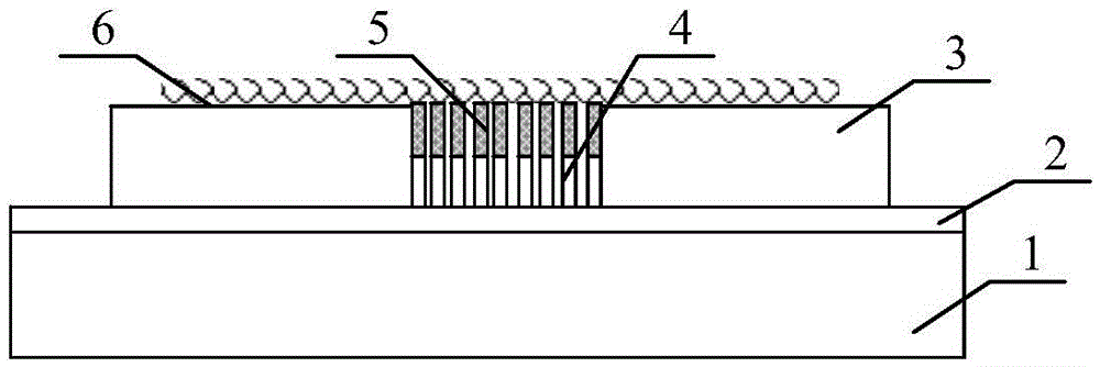
[0028] Such as figure 1 As shown, the homojunction photodetector with the vertical growth structure in this embodiment is provided with a bottom electrode 2 on the upper surface of the insulating substrate 1, and a mask layer 3 is arranged on the upper surface of the bottom electrode 2; The center of 3 is provided with a through hole communicating with the bottom electrode 2; perpendicular to the upper surface of the bottom electrode 2, an N-type semiconductor material 4 in an array structure is grown in the through hole, and an array structure is grown on the N-type semiconductor material 4 The P-type semiconductor material 5, the N-type semiconductor material 4 and the P-type semiconductor material 5 form a PN homojunction; a top electrode 6 is arranged above the mask layer 3, and the top electrode 6 does not exceed the boundary of the mask layer 3 and completely covers Through holes; the bottom electrode 2 and the N-type semiconductor material 4 , and the top electrode 6 an...
Embodiment 2
[0040] The homojunction photodetector of this embodiment has the same structure as that of Embodiment 1, the only difference is that the semiconductor material is MoS 2 . Its preparation method is as follows:
[0041] a. After ultrasonically cleaning the silicon wafer with a thickness of 300nm of silicon oxide on the surface, a layer of Au electrode with a thickness of about 50nm is vapor-deposited on the surface by means of electron beams.
[0042] b. Evaporating a layer of Al on the Au electrode by pulsed laser deposition 2 o 3 The insulating layer acts as a mask layer, and makes the Al 2 o 3 The center of the insulating layer is left with a 6cm diameter via as MoS 2 The deposition area; the area of the mask layer is about 4 / 5 of the Au electrode, and the thickness is about 200nm.
[0043] c. Attach a mask plate with a round hole in the middle on the silicon wafer where the Au electrode and insulating layer are evaporated. The position of the round hole corresponds t...
PUM
| Property | Measurement | Unit |
|---|---|---|
| Thickness | aaaaa | aaaaa |
| Thickness | aaaaa | aaaaa |
| Thickness | aaaaa | aaaaa |
Abstract
Description
Claims
Application Information


