Organic light-emitting diode and fabrication method thereof and organic light-emitting diode display panel

A technology of light-emitting diodes and manufacturing methods, applied in semiconductor/solid-state device manufacturing, electrical components, electric solid-state devices, etc., can solve problems such as reducing luminous efficiency, affecting device luminous efficiency and life, and electron and hole imbalance

Inactive Publication Date: 2016-06-01
SHENZHEN CHINA STAR OPTOELECTRONICS TECH CO LTD
View PDF5 Cites 0 Cited by
  • Summary
  • Abstract
  • Description
  • Claims
  • Application Information

AI Technical Summary

Problems solved by technology

[0003] Since the mobility of holes in OLEDs is usually several orders of magnitude higher than that of electrons, hole injection is also easier than electron injection, resulting in an imbalance of electrons and holes in OLEDs.
Excessive holes will migrate from the anode to the cathode to f...

Method used


Image

  • Organic light-emitting diode and fabrication method thereof and organic light-emitting diode display panel
  • Organic light-emitting diode and fabrication method thereof and organic light-emitting diode display panel

Examples


Embodiment Construction

[0018] In the following description, for purposes of illustration rather than limitation, specific details, such as specific system architectures, interfaces, and techniques, are set forth in order to provide a thorough understanding of the present invention.

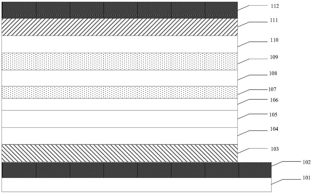
[0019] see figure 1 , figure 1 It is a schematic cross-sectional structure diagram of an embodiment of the organic light emitting diode of the present invention.

[0020] Such as figure 1 As shown, the organic light-emitting diode (OLED) in this embodiment includes a glass substrate 101, an anode metal layer 102 stacked on the glass substrate 101, a hole injection layer 103, a hole transport layer 104, an electron Blocking layer 105 , first light emitting layer 106 , second hole blocking layer 107 , second light emitting layer 108 , first hole blocking layer 109 , electron transport layer 110 , electron injection layer 111 , cathode metal layer 112 .

[0021] Wherein, the second hole blocking layer 107 is arranged be...


PUM


Abstract

The invention discloses an organic light-emitting diode and a fabrication method thereof and an organic light-emitting diode display panel. The organic light-emitting diode comprises a glass substrate, an anode metal layer, a hole injection layer, a hole transport layer, an electron blocking layer, a first light-emitting layer, a second hole blocking layer, a second light-emitting layer, a first hole blocking layer, an electron transport layer, an electron injection layer and a cathode metal layer, wherein the anode metal layer, the hole injection layer, the hole transport layer, the electron blocking layer, the first light-emitting layer, the second hole blocking layer, the second light-emitting layer, the first hole blocking layer, the electron transport layer, the electron injection layer and the cathode metal layer are stacked; the second blocking layer is used for slowing down the migration rate of holes injected from the hole injection layer toward the electron transport layer; and the holes and electrons injected from the electron injection layer form excitons and emit lights on the first light-emitting layer and the second light-emitting layer. In the manner, the organic light-emitting diode can effectively improve the luminous efficiency.

Description

technical field [0001] The invention relates to the field of field display, in particular to an organic light emitting diode, a manufacturing method thereof, and an organic light emitting diode display panel. Background technique [0002] Organic light-emitting diodes (organic light-emitting diode, OLED) have the characteristics of self-illumination. Displays made of OLEDs have a series of advantages such as high brightness, fast response, low energy consumption, and bendability. This is widely used in mobile phones, computers, PADs, digital Camcorder, TV, etc. [0003] Since the mobility of holes in OLEDs is usually several orders of magnitude higher than that of electrons, hole injection is also easier than electron injection, thus causing an imbalance of electrons and holes in OLEDs. Excessive holes will migrate from the anode to the cathode to form a leakage current, which affects the luminous efficiency and life of the device; when the holes migrate to the cathode, the...

Claims


Application Information

Patent Timeline
IPC IPC(8): H01L51/50H01L51/56
CPCH10K50/13H10K50/18H10K71/00
Inventor 徐超
Owner SHENZHEN CHINA STAR OPTOELECTRONICS TECH CO LTD
Why Eureka
Try Eureka