A Switched Capacitor Bias Circuit for Reduced Power Consumption in Operational Amplifiers

An operational amplifier and switched capacitor technology, applied in the field of microelectronics, to achieve the effects of speeding up signal transmission, reducing overhead and increasing power consumption

Active Publication Date: 2018-09-14
BEIJING MXTRONICS CORP +1
View PDF5 Cites 0 Cited by
  • Summary
  • Abstract
  • Description
  • Claims
  • Application Information

AI Technical Summary

Problems solved by technology

[0008] The technical problem of the present invention: overcomes the existing problems of the existing bias switch, and provides a switched capacitor bias circuit that can reduce the power consumption of the operational amplifier. The bias circuit utilizes capacitor voltage division to quickly transmit the input signal; The feed-through effect has little interference; different bias voltages can be generated without complex front-end bias generation circuits, saving chip area; no DC current path, no additional power consumption

Method used


Image

  • A Switched Capacitor Bias Circuit for Reduced Power Consumption in Operational Amplifiers
  • A Switched Capacitor Bias Circuit for Reduced Power Consumption in Operational Amplifiers
  • A Switched Capacitor Bias Circuit for Reduced Power Consumption in Operational Amplifiers

Examples


Embodiment Construction

[0031] The present invention will be explained below in conjunction with the accompanying drawings and specific embodiments.

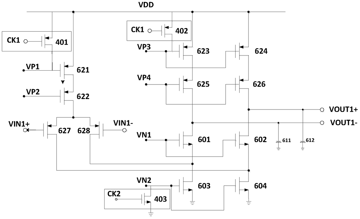
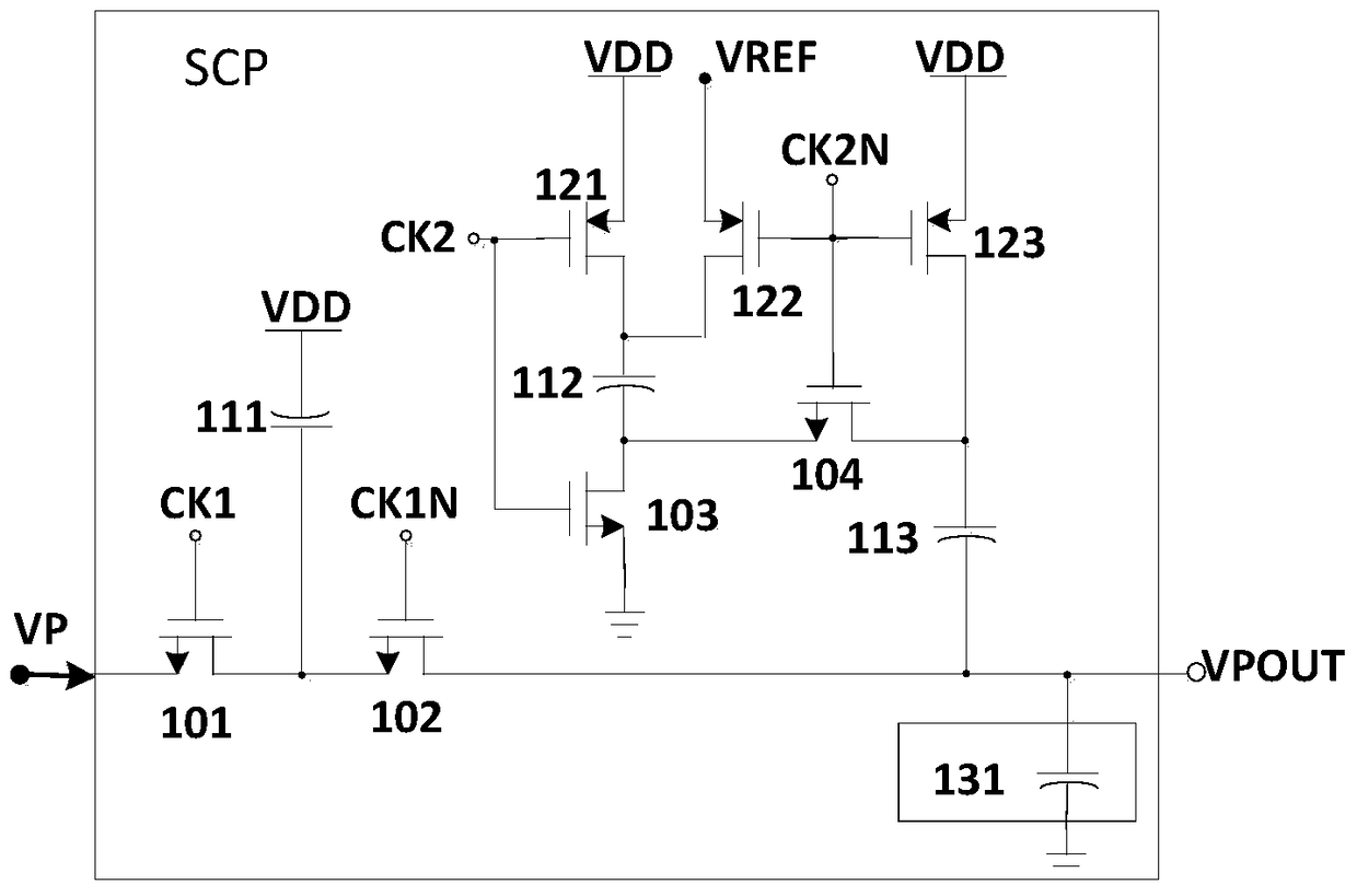
[0032] like image 3 As shown, the P-type current source transistor bias unit SCP in the present invention includes a first NMOS transistor 101, a second NMOS transistor 102, a third NMOS transistor 103, a fourth NMOS transistor 104, a first PMOS transistor 121, a second PMOS transistor Tube 122, third PMOS tube 123, first charge storage capacitor 111, second charge storage capacitor 112, third charge storage capacitor 113, first equivalent parasitic capacitor 131, first bias signal VP, second bias signal VREF;

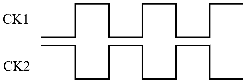
[0033] like Figure 5 As shown, the first clock signal CK1 and the third clock signal CK1N are two anti-phase non-overlapping clocks, the second clock signal CK2 and the fourth clock signal CK2N are two anti-phase non-overlapping clocks, the second clock signal CK2 and The first clock signal CK1 is in phase, and its pulse width is slightly ...


PUM


Abstract

The invention discloses a switched capacitor biasing circuit capable of reducing the power consumption of an operational amplifier. The switched capacitor biasing circuit comprises a P type current source tube biasing unit SCP and an N type current source tube biasing unit SCN. The biasing circuit utilizes the capacitor divider to transmit input signals quickly; the interference caused by the clock feedthrough effect is small; different biasing voltages can be generated without complex front-end bias generation circuit, thus the chip area is saved; and no direct current path is needed, so that no additional power consumption is increased. The switched capacitor biasing circuit can be widely applied to any operational amplification circuit working under certain switching frequency, and help the operational amplifier to achieve relatively low power consumption and quick signal establishment.

Description

technical field [0001] The invention belongs to the technical field of microelectronics and relates to a bias circuit of a high-performance operational amplifier, in particular to a switched capacitor bias circuit capable of effectively reducing the power consumption of the operational amplifier. Background technique [0002] As an intermediate bridge circuit between the analog world and the digital world, the analog-to-digital converter is widely used in wireless communication base stations, medical equipment, military radar and precision guidance systems, etc. With the increasing popularity of portable devices, it is required that the analog-to-digital converter has high speed and high precision, and can obtain lower power consumption at the same time. However, high-performance analog-to-digital converters often come at the expense of higher power consumption in order to obtain higher speed and accuracy. As the core unit and main source of power consumption in the analog-...

Claims


Application Information

Patent Timeline
Patent Type & Authority Patents(China)
IPC IPC(8): H03F3/45
CPCH03F3/4539H03F2203/45092
Inventor 李雪赵元富文治平王宗民周亮冯文晓张硕
Owner BEIJING MXTRONICS CORP
Why Eureka
Try Eureka