A kind of multilayer pcb circuit board

A PCB circuit board and substrate technology, which is applied in the direction of circuit devices, printed circuits, printed circuits, etc., can solve the problems of poor performance of multi-layer PCB circuit boards, degradation of electronic product performance, and difficult-to-stack structure symmetry, etc., to achieve electromagnetic compatibility performance Excellent, balanced performance, and performance-enhancing effects

Active Publication Date: 2018-05-18
PUTIAN HANJIANG YD PCB CO LTD
View PDF10 Cites 0 Cited by
  • Summary
  • Abstract
  • Description
  • Claims
  • Application Information

AI Technical Summary

Problems solved by technology

After the number of layers is determined, determine the location of the internal electrical layer and how to distribute different signals on these layers. This is a design problem for the multilayer PCB stack structure. The stack structure is an important factor affecting the EMC performance of the PCB board. It is also An important technical means to suppress electromagnetic interference, because if the EMC performance of the multi-layer PCB circuit board is not good, or the electromagnetic interference is large, it will seriously affect the transmission of the signal, which will undoubtedly lead to a sharp decline in the performance of electronic products!
[0004] Although the multi-layer PCB circuit board technology has developed to a certain extent nowadays, when each manufacturer produces a multi-layer PCB circuit board, it must comprehensively consider various factors when designing the stacked structure of the multi-layer PCB circuit board. A substantial balance is achieved in terms of wiring, number of layers, cost, and stacked structure symmetry, and as the number of circuit board layers increases, the arrangement and combination of signal layers, ground layers, and power layers increases. Determining an optimal combination method has become a headache for multilayer PCB circuit board manufacturers

Method used


Image

  • A kind of multilayer pcb circuit board
  • A kind of multilayer pcb circuit board
  • A kind of multilayer pcb circuit board

Examples


Embodiment 1

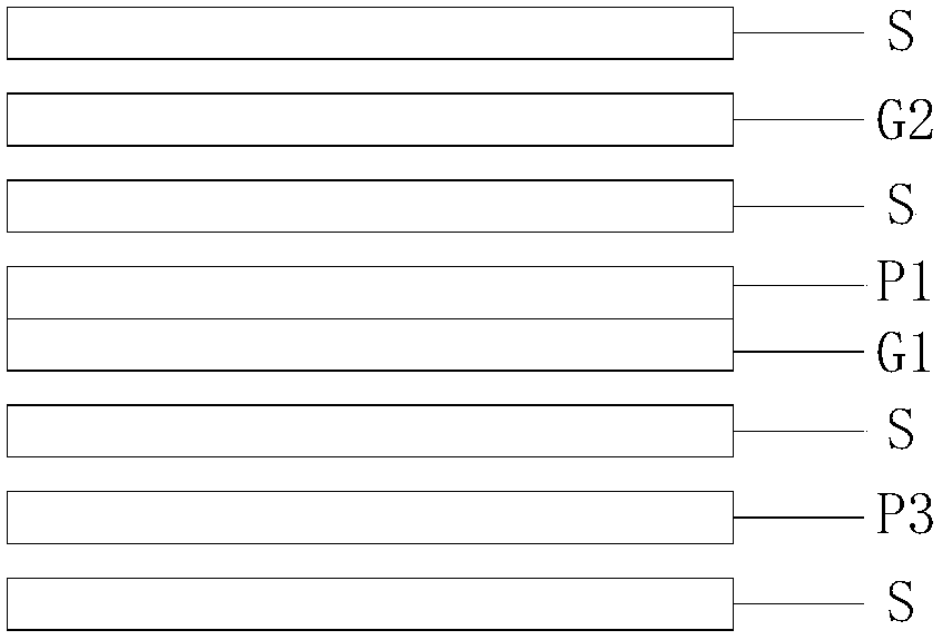
[0029] Such as figure 1 As shown, the total number of layers of the PCB circuit board is 8 layers, and from top to bottom are the signal layer S, the second ground layer G2, the signal layer S, the first power layer P1, the first ground layer G1, the signal layer S, the third power layer P3 and the signal layer S.

[0030] The thickness of the PCB circuit board is 1.2-2.4mm.

Embodiment 2

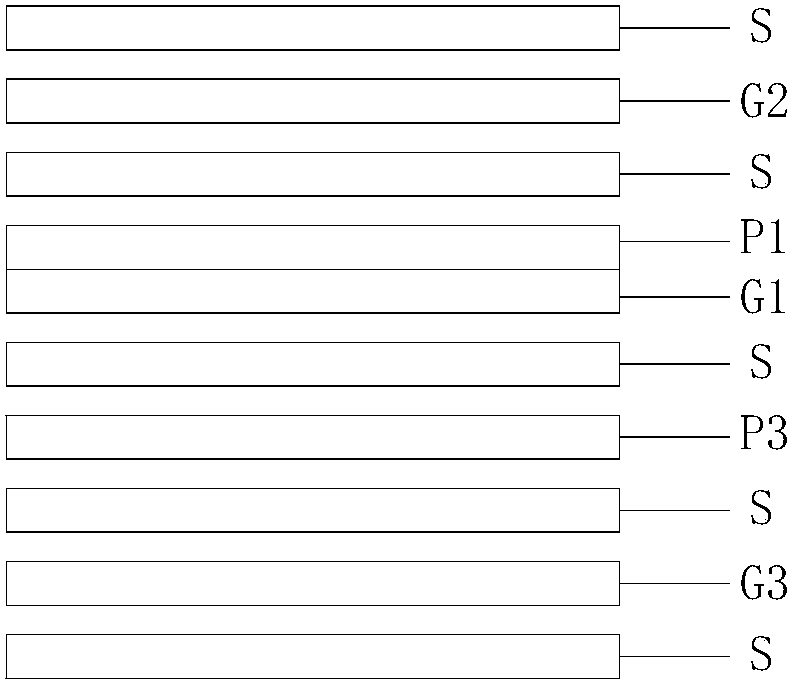
[0032] Such as figure 2 As shown, the total number of layers of the PCB circuit board is 10 layers, which are the signal layer S, the second ground layer G2, the signal layer S, the first power layer P1, the first ground layer G1, and the signal layer from top to bottom. S, the third power layer P3, the signal layer S, the third ground layer G3 and the signal layer S.

[0033] The thickness of the PCB circuit board is 1.6-3.2mm.

Embodiment 3

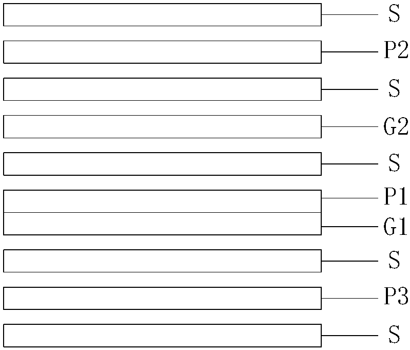
[0035] Such as image 3 As shown, the total number of layers of the PCB circuit board is 10 layers, which are the signal layer S, the second power layer P2, the signal layer S, the second ground layer G2, the signal layer S, and the first power layer from top to bottom. P1, the first ground layer G1, the signal layer S, the third power layer P3 and the signal layer S.

[0036] The thickness of the PCB circuit board is 1.6-3.2mm.


PUM


Abstract

The invention relates to a multilayer PCB circuit board, and the total layer number is an even number which is not smaller than 8. The multilayer PCB circuit board comprises a base board, and the base board comprises a first power supply layer and a first grounding layer which are vertically arranged; multiple second grounding layers and multiple second power supply layers are sequentially distributed on the upper surface of the first power supply layer from bottom to top in a staggered mode, and multiple third power supply layers and multiple third grounding layers are sequentially distributed on the lower surface of the first grounding layer from top to bottom in a staggered mode; a signal layer is arranged between the first power supply layer and the second grounding layer adjacent to the first power supply layer, between each second grounding layer and the corresponding second power supply layer adjacent to the second grounding layer, between the first grounding layer and the third power supply layer adjacent to the first grounding layer, between each third power supply layer and the corresponding third grounding layer adjacent to the third power supply layer, on the upper surface of the uppermost layer and on the lower surface of the lowermost layer. The multilayer PCB circuit board is reasonable in design, excellent in electromagnetic compatibility and high in anti-electromagnetic interference and signal transmission capacity, all the properties are more balanced, and the properties of electronic products are greatly promoted.

Description

technical field [0001] The invention relates to the technical field of circuit boards, in particular to a multilayer PCB circuit board. Background technique [0002] With the continuous development of surface mount technology (SMT) and the continuous introduction of a new generation of surface mount devices (SMD), such as QFP, QFN, CSP, BGA (especially MBGA), electronic products are more intelligent and miniaturized, so It has promoted major reforms and advancements in printed circuit board (PCB) industrial technology. Printed circuit board (PCB), as the carrier of various electronic devices such as chips, is developing in the direction of high density, high speed, low power consumption, low cost and green environmental protection. [0003] When designing a multilayer PCB circuit board, it is necessary to determine the circuit board structure used according to the scale of the circuit, the size of the circuit board and the requirements of electromagnetic compatibility (EMC)...

Claims


Application Information

Patent Timeline
Patent Type & Authority Patents(China)
IPC IPC(8): H05K1/02
CPCH05K1/0218H05K1/0298H05K2201/09327
Inventor 刘胜贤罗光俊唐瑞芳
Owner PUTIAN HANJIANG YD PCB CO LTD
Why Eureka
Try Eureka