FPGA wiring method and device

A wiring method and wiring device technology, applied in CAD circuit design, special data processing applications, instruments, etc., can solve problems such as insufficient FPGA wiring scheme

Inactive Publication Date: 2016-06-15
SHENZHEN PANGO MICROSYST CO LTD
View PDF4 Cites 0 Cited by
  • Summary
  • Abstract
  • Description
  • Claims
  • Application Information

AI Technical Summary

Problems solved by technology

[0009] The present invention provides an FPGA wiring method and device, which solves the problem that the existing FPGA wiring scheme is not perfect enough

Method used


Image

  • FPGA wiring method and device
  • FPGA wiring method and device
  • FPGA wiring method and device

Examples


Embodiment Construction

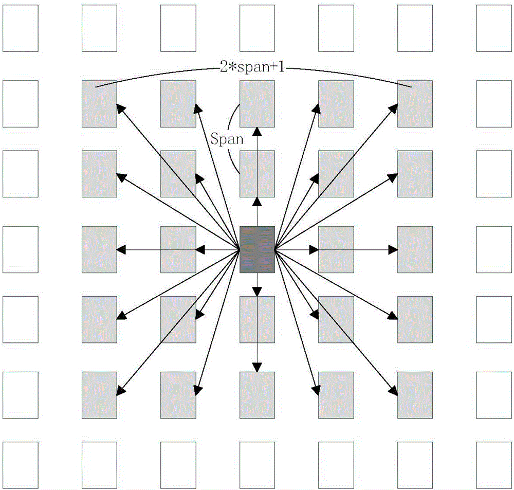
[0037] In the present invention, the cost may be a single factor such as delay, path, conflict, or a combination of multiple factors. The cost estimation model can be in the form of a list, and the router loads the list when starting the routing, parses it and stores it in the hash table, that is, realizes the cost value estimation between nodes based on the look-up table.

[0038] The concept of the present invention will be further described in detail through specific embodiments below.

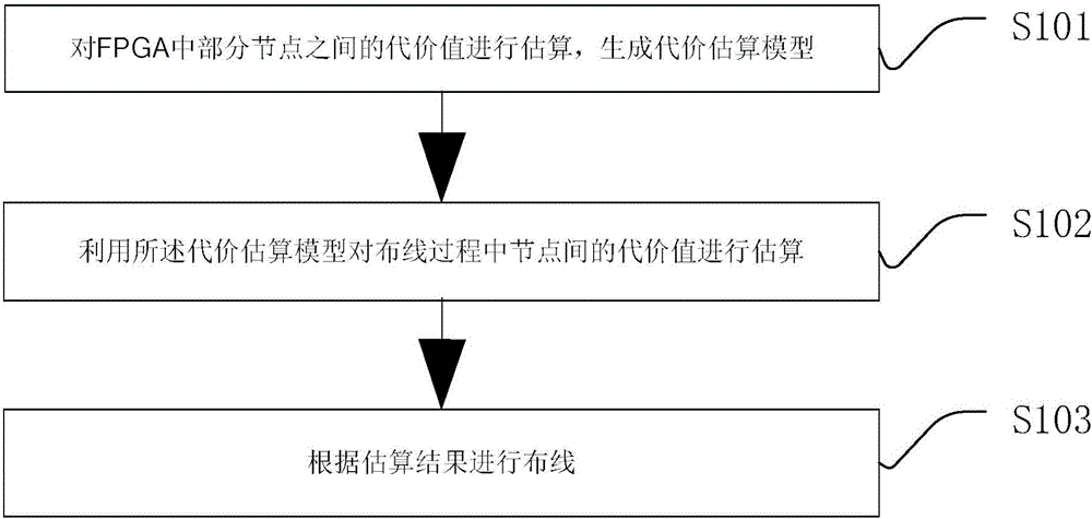
[0039] Such as figure 2 As shown, the flow chart of the FPGA wiring method provided by an embodiment of the present invention mainly includes the following steps:

[0040] S101. Estimate the cost value between some nodes in the FPGA, and generate a cost estimation model;

[0041] S102. Using the cost estimation model to estimate the cost value between nodes in the wiring process;

[0042] S103. Perform wiring according to the estimation result.

[0043] Step S101 includes but is not li...


PUM


Abstract

The invention discloses an FPGA wiring method and device. The method comprises the steps that a cost value between part of nodes in an FPGA is estimated, and a cost estimating model is generated; the cost estimating model is utilized for estimating the cost value between the nodes in the wiring process; wiring is carried out according to the estimation result. According to the technical scheme, the problem that an existing FPGA wiring scheme is not perfect enough is solved.

Description

technical field [0001] The invention relates to the technical field of field programmable gate array (FPGA), in particular to an FPGA wiring method and device. Background technique [0002] Since the advent of FPGA, its unique programmability has greatly simplified the process of traditional digital circuit design, and more and more electronic designers use FPGA chips to design electronic systems. As the scale of FGPA continues to expand, the performance requirements for software algorithms are also getting higher and higher. For example, a larger scale means a larger layout span and a more complex circuit netlist, which puts higher requirements on FPGA routing efficiency. Therefore, how to reduce the routing time to a minimum without affecting the performance becomes a factor that cannot be ignored in the routing algorithm. [0003] At present, the more common wiring algorithm is the A* algorithm, which uses the concept of cost function. Such as figure 1 In the node arr...

Claims


Application Information

Patent Timeline
IPC IPC(8): G06F17/50
CPCG06F30/39
Inventor 夏炜
Owner SHENZHEN PANGO MICROSYST CO LTD
Why Eureka
Try Eureka