Manufacturing method for terminal structure of trench IGBT device

A manufacturing method and terminal structure technology, applied in semiconductor/solid-state device manufacturing, semiconductor devices, electrical components, etc., can solve the difficulty of process control, the limitation of the depth of the charge storage layer and the maximum doping concentration, and the problem of the P well of the charge storage layer influence and other issues, to achieve the effect of reducing the instability of device performance

Inactive Publication Date: 2016-06-15
SHANGHAI DAOZHI TECH CO LTD
View PDF3 Cites 9 Cited by
  • Summary
  • Abstract
  • Description
  • Claims
  • Application Information

AI Technical Summary

Problems solved by technology

The charge storage layer is usually formed by ion implantation and diffusion methods. The charge storage layer formed by this method is easily affected by

Method used


Image

  • Manufacturing method for terminal structure of trench IGBT device

Examples


Embodiment

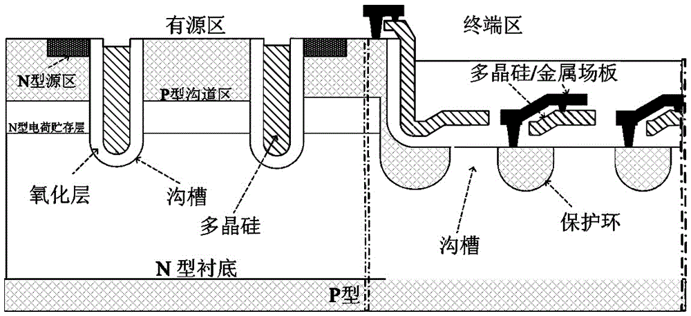
[0020] Example: figure 1 As shown, the manufacturing method of the present invention is fully compatible with other trench IGBT devices, and only one step of photolithography process is needed.

[0021] First, an N-type epitaxial layer is grown on a selected N-type epitaxial silicon substrate or a region fuse to form a charge storage layer, and a P-type epitaxial layer is grown on it to form a channel region. Photolithography terminal area trench pattern, dry etching silicon substrate, growing field oxide layer; photolithography active area and etching field oxide layer; photolithography terminal area protection ring, implanting P-type impurities and diffusing to form an effective protective ring. Photoetching the gate trench in the active area, etching the trench and growing a gate oxide layer, depositing in-situ doped polysilicon material to fill the trench; then photoetching the gate pattern and terminal protection field plate, and etching the polysilicon; Photoetching th...


PUM


Abstract

A manufacturing method for a terminal structure of a trench IGBT device is disclosed. The manufacturing method comprises the steps of growing an N type epitaxial part on an N type epitaxial silicon substrate or a regional fuse piece to form a charge storage region with certain doping concentration and thickness; continuing to grow a P type epitaxial part to form a channel region with an MOS-structured top layer; photoetching a terminal region trench pattern, dry etching the silicon substrate and growing a field oxide layer; photoetching an active region and etching the field oxide layer; photoetching a terminal region protection ring, and injecting P type impurities and enabling the impurities to be diffused to form an active protection ring; photoetching an active region gate trench, etching the trench and growing a gate oxide layer; depositing an in-situ-doped polysilicon material to fill the trench; then photoetching the gate pattern and a terminal protection field board, and etching the polysilicon; photoetching an N type source region and injecting N type impurities, then depositing the oxide layer or silicon nitride and other insulating materials, and performing annealing and compacting, photoetching contact holes, and etching the insulating layer to expose P well regions and N type source region silicon surfaces of all the pre-formed cells.

Description

technical field [0001] The invention relates to a method for manufacturing a terminal structure of a trench IGBT device, and belongs to the technical field of manufacturing power semiconductor devices. Background technique [0002] As the main representative of new power semiconductor devices, IGBTs are widely used in the fields of industry, information, new energy, medicine, transportation, military and aviation. At present, the withstand voltage of IGBT devices on the market is as high as 6500V, the current of a single die is as high as 200A, and the frequency is as high as 300KHz. In the field of high frequency and high power, there is no other device that can replace it. With the continuous advancement of semiconductor materials and processing technology, IGBT devices using trench technology have become mainstream products. At the same time, the requirements for the electrical performance of trench IGBT devices are getting higher and higher. [0003] In order to reduc...

Claims


Application Information

Patent Timeline
IPC IPC(8): H01L21/331H01L21/20
CPCH01L29/66325H01L21/20
Inventor 汤艺永福王良元徐泓
Owner SHANGHAI DAOZHI TECH CO LTD
Why Eureka
Try Eureka