
Silicon through hole structure-based metal filling method and silicon through hole structure

A technology of through-silicon vias and metals, applied in the field of three-dimensional integrated circuits, can solve problems such as circuit breaks, achieve the effects of avoiding circuit breaks, shortening the length of connections, and improving system integration

Inactive Publication Date: 2016-06-15
INST OF MICROELECTRONICS CHINESE ACAD OF SCI
View PDF7 Cites 1 Cited by
  • Summary
  • Abstract
  • Description
  • Claims
  • Application Information

AI Technical Summary

Problems solved by technology

[0005] The present invention solves the technical problem of circuit disconnection caused by the notch effect in the prior art by providing a metal filling method based on a through-silicon via structure and a through-silicon via structure.

Method used


Image

  • Silicon through hole structure-based metal filling method and silicon through hole structure
  • Silicon through hole structure-based metal filling method and silicon through hole structure
  • Silicon through hole structure-based metal filling method and silicon through hole structure

Examples


Embodiment Construction

[0048] In order to solve the technical problem of circuit disconnection caused by the notch effect in the three-dimensional integrated circuit in the prior art, the present invention provides a metal filling method based on a through-silicon via structure and a through-silicon via structure.

[0049] In order to make the purpose, technical solutions and advantages of the embodiments of the present invention clearer, the technical solutions in the embodiments of the present invention will be clearly and completely described below in conjunction with the drawings in the embodiments of the present invention. Obviously, the described embodiments It is a part of embodiments of the present invention, but not all embodiments. Based on the embodiments of the present invention, all other embodiments obtained by persons of ordinary skill in the art without creative efforts fall within the protection scope of the present invention.

[0050] An embodiment of the present invention provides...


PUM

PropertyMeasurementUnit
thicknessaaaaaaaaaa
thicknessaaaaaaaaaa

Abstract

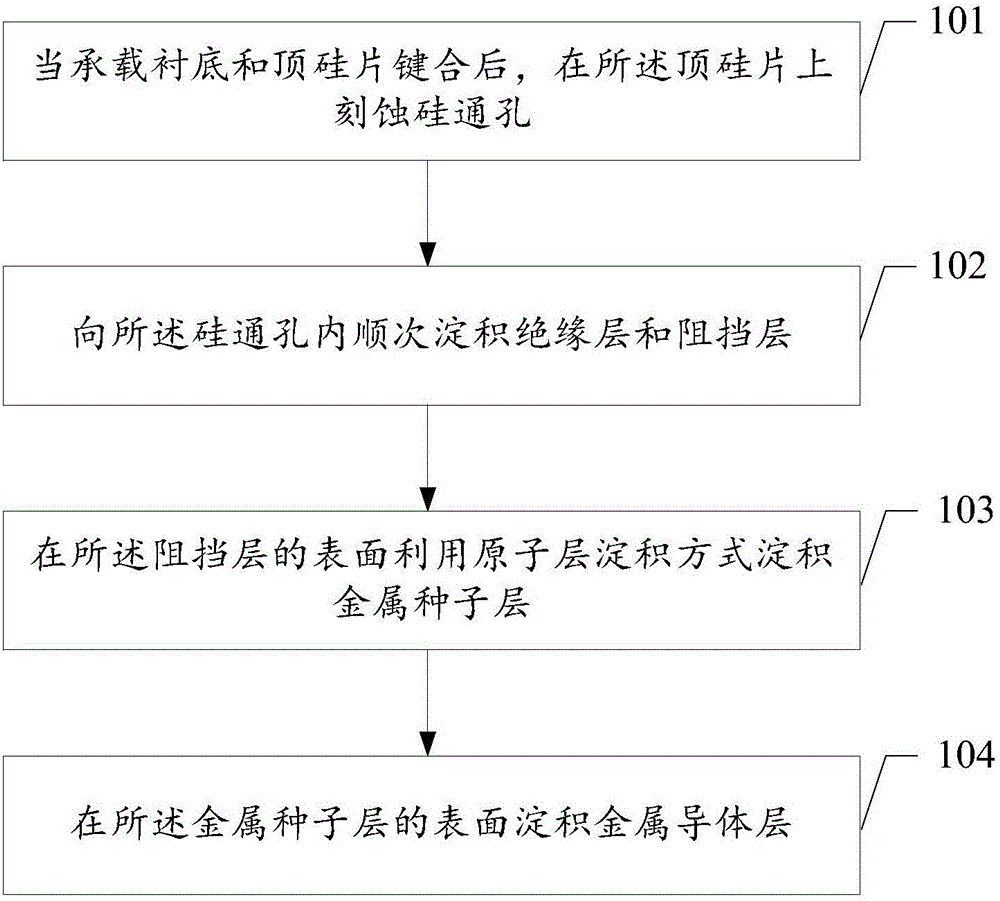
The invention relates to the technical field of three-dimensional integrated circuits, in particular to a silicon through hole structure-based metal filling method and a silicon through hole structure. The method comprises the following steps: after bonding a bearing substrate and a top silicon wafer, etching a silicon through hole on the top silicon wafer; sequentially depositing an insulating layer and a barrier layer in the silicon through hole; depositing a metal seed layer on the surface of the barrier layer in an atomic layer deposition manner; and depositing a metal conductor layer on the surface of the metal seed layer. The metal seed layer is added between the barrier layer and the metal conductor layer, so that circuit disconnection caused by a conductor fault can be avoided; and meanwhile, the condition that deposition of the metal seed layer has good surface coverage on any shape and form is achieved in the atomic layer deposition manner; the condition that the surface of the barrier layer can completely cover the metal seed layer is ensured; the circuit disconnection caused by the conductor fault is further avoided; and the process reliability of metal filling is improved.

Description

technical field [0001] The invention relates to the technical field of three-dimensional integrated circuits, in particular to a metal filling method based on a through-silicon via structure and a through-silicon via structure. Background technique [0002] At present, the three-dimensional integration technology based on through-silicon via (Through Silicon Vias, TSV) interconnection is a new direction of research and development in the semiconductor field. Among them, the three-dimensional integrated circuit adopts a three-dimensional stacking method, so it can integrate micro-electromechanical systems (MicroElectroMechanicalSystem, MEMS), radio frequency modules, memory and processors into one system, which greatly improves the integration of the system and reduces packaging. The size and weight of the body increase the packaging density, so that the most components can be accommodated per unit volume, and the form factor is reduced. Moreover, the interconnection and com...

Claims


Application Information

Patent Timeline
Patent Type & Authority Applications(China)
IPC IPC(8): H01L21/768H01L23/48
CPCH01L21/76898H01L23/481
Inventor 云世昌焦斌斌王桂磊孔延梅张乐民俞利民陈大鹏
Owner INST OF MICROELECTRONICS CHINESE ACAD OF SCI
Learn More