

Array substrate, method for manufacturing same and display device
A technology for array substrates and display areas, applied in nonlinear optics, instruments, optics, etc., can solve the problems of insufficient contact between the source and drain electrodes and the active layer, easy to form open circuits, and unstable contact, etc., to ensure display Quality, avoiding circuit breaks, and ensuring quality effects
- Summary
- Abstract
- Description
- Claims
- Application Information
AI Technical Summary
Problems solved by technology
Method used
Image

Examples
Embodiment 1
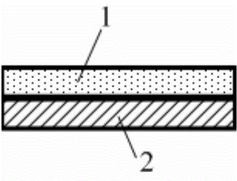
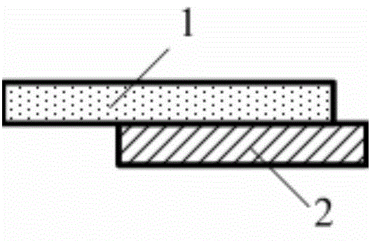
[0035] This embodiment provides an array substrate, including a base substrate and a plurality of electrode structures arranged on the base substrate, such as figure 1 and figure 2 As shown, the electrode structure includes a body electrode 1 made of metal material, and the electrode structure also includes a substrate electrode 2, which is made of a transparent metal oxide material; the substrate electrode 2 is located below the body electrode 1, and In the orthographic projection direction, it partially overlaps with the body electrode 1 (such as figure 2 ) or completely overlapping (as in figure 1 ); the substrate electrode 2 is electrically connected to the body electrode 1 .
[0036] In this embodiment, the body electrode 1 and the substrate electrode 2 completely overlap in the orthographic projection direction.
[0037] Among them, the metal material for making the body electrode 1 includes chromium, molybdenum, aluminum, copper, neodymium aluminum alloy or aluminu...
Embodiment 2
[0060] This embodiment provides an array substrate. The difference from Embodiment 1 is that on the basis of Embodiment 1, a spare electrode is provided in the display area of the array substrate, and the body electrode also includes a spare electrode, and the substrate electrode and the display electrode (that is, the pixel electrodes) are formed using the same material and in the same patterning process. That is, the substrate electrode under the spare electrode and the pixel electrode are formed in the same layer of the array substrate.
[0061] Wherein, the spare electrode and the data line are made of the same material and formed on the same layer in the same patterning process, and the spare electrode is generally used to repair a short-circuited or disconnected data line.
[0062] Other structures of the array substrate in this embodiment are the same as those in Embodiment 1, and will not be repeated here.
[0063] The preparation of the array substrate only needs t...
Embodiment 3
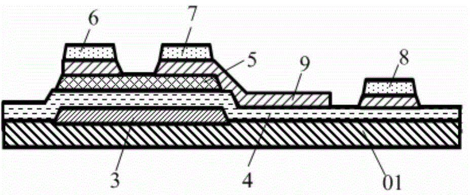
[0065] This embodiment provides an array substrate, which is different from Embodiment 1-2, as Figure 4 As shown, on the basis of Example 2, the gate insulating layer 4 also extends to the non-display area at the same time; the electrode structure is also arranged in the non-display area, and the signal input electrode 11 is also arranged above the gate insulating layer 4 extending to the non-display area , the body electrode also includes a signal input electrode 11 , and the substrate electrode and the display electrode (ie, the pixel electrode 9 ) are made of the same material and formed in the same patterning process. That is, the substrate electrode under the signal input electrode 11 and the pixel electrode 9 are formed in the same layer of the array substrate.
[0066] Wherein, the signal input electrodes 11 and the data lines 8 are made of the same material, and are formed on the same layer in the same patterning process.
[0067] The signal input electrodes 11 inclu...
PUM
| Property | Measurement | Unit |
|---|---|---|
| Thickness | aaaaa | aaaaa |
| Thickness | aaaaa | aaaaa |
| Thickness | aaaaa | aaaaa |
Abstract
Description
Claims
Application Information