

Thin-film bulk acoustic resonator and manufacturing method thereof
A thin-film bulk acoustic wave and manufacturing method technology, applied in electrical components, impedance networks, etc., can solve problems such as increased material cost and device reliability deterioration, and achieve the effects of improving reliability, avoiding damage, and reflecting environmental friendliness
- Summary
- Abstract
- Description
- Claims
- Application Information
AI Technical Summary
Problems solved by technology
Method used
Image


Examples
Embodiment Construction
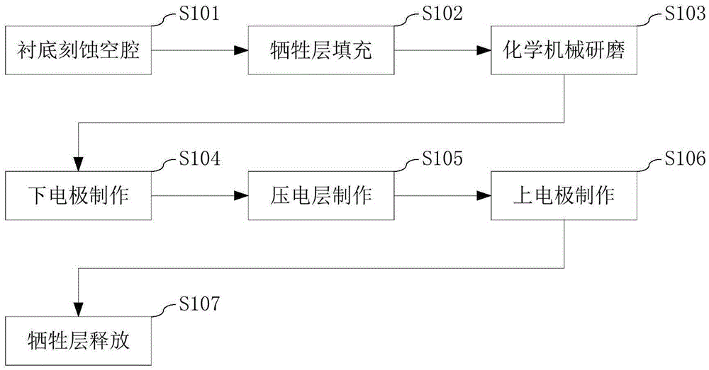
[0028] The first embodiment of the FBAR manufacturing method of the present application includes the following steps:
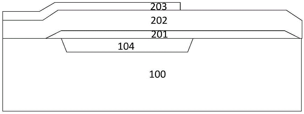
[0029] Step S301, please refer to Figure 3a , A support layer 101 is deposited on the substrate 100. The support layer 101 may be an insulating material such as silicon dioxide, silicon nitride, silicon oxynitride, or the like.
[0030] Step S302, please refer to Figure 3b The support layer 101 is etched to form the cavity 104, for example, using photolithography and etching processes. The cavity 104 is also connected with a sacrificial layer release channel (not shown) that is etched together.
[0031] Step S303, please refer to Figure 3c A sacrificial layer 105 is deposited on the substrate 100 and the supporting layer 101, and the sacrificial layer 105 fills the cavity 104 and the sacrificial layer release channel. The sacrificial layer 105 is, for example, black diamond (Black Diamond), photoresist (Photoresist), polyimide (Polyimide), etc., which can be et...
PUM
 Abstract
Description
Claims
Application Information