Method for optimizing FPGA (Field-Programmable Gate Array) chip layout based on area clock

A regional clock and chip layout technology, applied in the direction of logic circuits using basic logic circuit components, logic circuits using specific components, etc., can solve problems such as setup time violations, hold time violations, timing violations, etc., to achieve FPGA layout optimization, Effect of reducing wiring length and improving layout

Active Publication Date: 2016-06-15
CAPITAL MICROELECTRONICS
View PDF2 Cites 7 Cited by
  • Summary
  • Abstract
  • Description
  • Claims
  • Application Information

AI Technical Summary

Problems solved by technology

[0004] However, the actual physical positions of the regs that make up these modules can be scattered anywhere in the FPGA chip. If the physical positions of two regs driven by the same regional clock are far apart, or although the physical positions are very close, they are connected to the clock respectively. When the wiring length of the driving end is very different, it will cause the delay of the clock signal to reach each reg to be different, that is to say, there is a clock skew (skew) between the clock signals of different receiving ends.
Clock skew will affect the synchronization of digital integrated circuits, which may cause two timing violations: hold time violation and setup time violation
Hold time violation means that the data signal is connected to the target register and fails to hold for a long enough time after the arrival of the valid edge, which will cause the data to not be correctly latched in the target register.

Method used


Image

  • Method for optimizing FPGA (Field-Programmable Gate Array) chip layout based on area clock
  • Method for optimizing FPGA (Field-Programmable Gate Array) chip layout based on area clock
  • Method for optimizing FPGA (Field-Programmable Gate Array) chip layout based on area clock

Examples


Embodiment Construction

[0025] In order to make the purpose, technical solution and advantages of the present invention clearer, the present invention will be further described in detail below in conjunction with the accompanying drawings. Obviously, the described embodiments are only some of the embodiments of the present invention, rather than all of them. Based on the embodiments of the present invention, all other embodiments obtained by persons of ordinary skill in the art without creative efforts fall within the protection scope of the present invention.

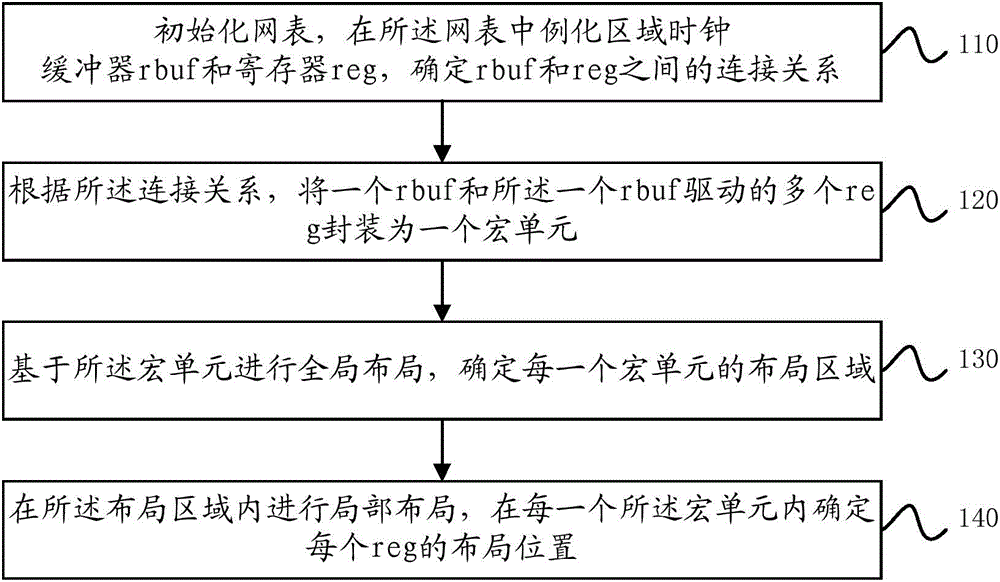
[0026] figure 1 An embodiment of the present invention provides a flow chart of a method for optimizing a local layout of an FPGA chip. As shown in the figure, the method includes the following steps:

[0027] Step 110, initialize the netlist, instantiate the regional clock buffer (rbuf) and register (reg) in the netlist, determine the connection relationship between rbuf and reg;

[0028] Specifically, in electronic circuit design, a netli...


PUM


Abstract

The invention relates to a method for optimizing FPGA chip layout based on an area clock. The method comprises following steps: initializing a netlist; instantiating area clock buffers (rbufs) and registers (regs); determining the connection relationships between the rbufs and the regs; packaging one rbuf and multiple regs driven by the rbuf into a macrocell according to the connection relationships; carrying out global layout based on the macrocells; determining the layout area of each macrocell; carrying out partial layout in the layout area; and determining the layout location of each reg in each macrocell. According to the method provided by the invention, the physical locations of the registers driven by the same area clock can be arranged in a relatively small area; the FPGA layout is optimized; the wiring length of the follow-up clock line is reduced; the wiring performance is improved; and the power consumption of the FPGA chips is reduced.

Description

technical field [0001] The invention relates to the technical field of integrated circuits, in particular to a method for optimizing field-programmable gate array (Field-Programmable Gate Array, FPGA) chip layout based on a regional clock. Background technique [0002] FPGA is a logic device with abundant hardware resources, powerful parallel processing capability and flexible reconfigurable capability. These features make FPGA more and more widely used in data processing, communication, network and many other fields. [0003] The clock inside the FPGA is divided into multiple regions. In this region, there are specific clocks that can drive the clock terminals of registers (reg) and random access memory (RandomAccessMemory, RAM). In the FPGA, these clocks are connected by dedicated clock lines of the clock tree. The global clock path of the FPGA requires a dedicated clock driver - a global clock buffer (GlobalClockbuffer, GBUF), and the clock signal can only drive the glo...

Claims


Application Information

Patent Timeline
IPC IPC(8): H03K19/177
Inventor 蒋中华黄攀吴鑫靳松
Owner CAPITAL MICROELECTRONICS
Why Eureka
Try Eureka