
Material with quantization abnormal Hall effect and Hall device formed by same

An anomalous Hall effect, quantized technology, applied in the field of condensed matter physics

Inactive Publication Date: 2016-06-22
INST OF PHYSICS - CHINESE ACAD OF SCI
View PDF6 Cites 9 Cited by
  • Summary
  • Abstract
  • Description
  • Claims
  • Application Information

AI Technical Summary

Problems solved by technology

Although V-doped samples show more superior properties than Cr-doped samples, but, like the quantum Hall effect, the perfect quantum anomaly can only be observed at extremely low temperatures (xx =0Ω, lateral resistivity ρ yx =25812.807557(±18)Ω, where "±18" means the error range of the last two digits)

Method used

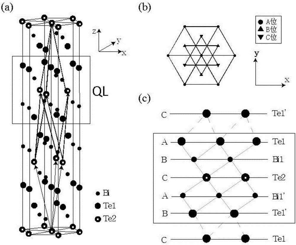
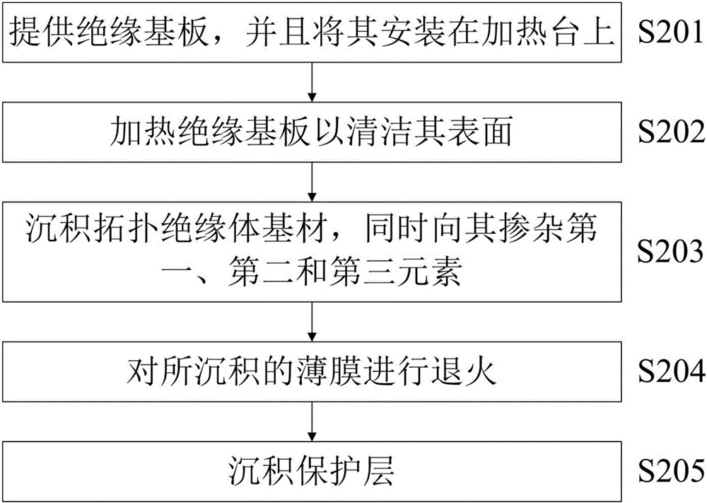
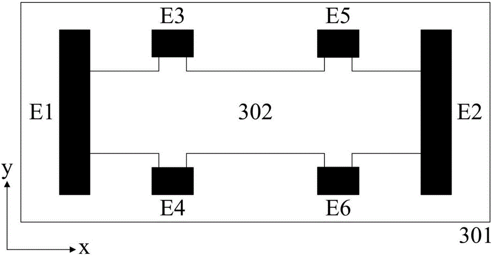

Image

  • Material with quantization abnormal Hall effect and Hall device formed by same
  • Material with quantization abnormal Hall effect and Hall device formed by same
  • Material with quantization abnormal Hall effect and Hall device formed by same

Examples


example 1

[0061] Example 1 (5QL thickness (Cr y V 1-y ) z (Bi x Sb 1-x ) 2-z Te 3 sample, where x=0.33, y=0, z=0.19, T=1.5K)

[0062] The sample of Example 1 is 5QL thick (Cr 0 V 1 ) 0.19 (Bi 0.33 Sb 0.67 ) 1.81 Te 3 , the insulating substrate is strontium titanate of 2mm×5mm×0.5mm. The magnetically doped topological insulator quantum well film is regulated through the bottom gate, and the maximum anomalous Hall resistance value of the film at a temperature of 1.5K can be obtained, please refer to Figure 4 and Figure 5 . At a temperature of 1.5K, the maximum value of the abnormal Hall resistance can be found through the regulation of the bottom gate voltage Vg. It can be seen that at a temperature of 1.5K, the Hall effect of the magnetically doped topological insulator quantum well thin film has a significant The hysteresis loop shows good ferromagnetism, the remanence ratio is 100%, and the anomalous Hall resistance can reach 21.24kΩ. However, it can be seen that the...

example 2

[0063] Example 2 (5QL thickness (Cr y V 1-y ) z (Bi x Sb 1-x ) 2-z Te 3 sample, where x=0.37, y=0.05, z=0.19, T=1.5K)

[0064] The double magnetic doping topological insulator quantum well film of example 2 is (Cr 0.05 V 0.95 ) 0.19 (Bi 0.37 Sb 0.63 ) 1.81 Te 3 , the insulating substrate is strontium titanate of 2mm×5mm×0.5mm. The maximum anomalous Hall resistance value of the film at a temperature of 1.5K can be obtained by regulating the double magnetically doped topological insulator quantum well film through the bottom gate. see Image 6 , at a temperature of 1.5K, the maximum value of the abnormal Hall resistance can be found through the regulation of the bottom gate voltage. It can be seen that at a temperature of 1.5K, the Hall effect of the double magnetically doped topological insulator quantum well film appears obvious The hysteresis loop shows good ferromagnetism, the remanence ratio is 100%, and the anomalous Hall resistance can reach 22.65kΩ. It ca...

example 3

[0065] Example 3 (5QL thickness (Cr y V 1-y ) z (Bi x Sb 1-x ) 2-z Te 3 samples where x=0.48, y=0.16, z=0.19, T=1.5K and 0.3K)

[0066] The dual magnetic doping topological insulator quantum well film of example 3 is (Cr 0.16 V 0.84 ) 0.19 (Bi 0.48 Sb 0.52 ) 1.81 Te3 , the insulating substrate is strontium titanate of 2mm×5mm×0.5mm. By regulating the double magnetically doped topological insulator quantum well film through the bottom gate, we can obtain the maximum anomalous Hall resistance value of the film at a temperature of 1.5K. see Figure 8 , at a temperature of 1.5K, through the adjustment of the bottom gate voltage, the maximum value of its abnormal Hall resistance was found. It can be seen that at a temperature of 1.5K, the Hall effect of the double magnetic doped topological insulator quantum well film appeared obvious The hysteresis loop shows good ferromagnetism, the remanence ratio is 100%, and the abnormal Hall resistance can reach 25.08kΩ (0.97h / e...


PUM


Abstract

The invention relates to a material with the quantization abnormal Hall effect and a Hall device formed by the same.In an embodiment, the material with the quantization abnormal Hall effect can comprise a topological insulator substrate, a first element doped into the topological insulator substrate, a second element and a third element.An electronic current carrier is introduced into the first element.The second element and the second element are doped into the topological insulator substrate.A hole type current carrier and magnetism are introduced into each of the second element and the second element.Therefore, a double-magnetism doped topological insulator is formed.

Description

technical field [0001] The invention generally relates to the field of condensed matter physics, and more particularly relates to a material capable of exhibiting quantized anomalous Hall effect at relatively high temperature, and a Hall device formed by using the material. Background technique [0002] Hall (EdwinH.Hall) discovered in 1879 that when a conductor with a longitudinal current is placed in a vertical magnetic field, a voltage value will be observed in the transverse direction of the current. This phenomenon is called the Hall by later generations. Hall effect (Hall effect, HE) (see Non-Patent Document 1). It is now known that the Hall effect is the deflection of electrons due to the Lorentz force when they move in a magnetic field, thereby forming charge accumulation on both sides perpendicular to the direction of the current to form a lateral voltage, so that the subsequent electrons are subjected to an electric field force After balancing with the Lorentz for...

Claims


Application Information

Patent Timeline
Patent Type & Authority Applications(China)
IPC IPC(8): H01L43/10H01L43/06H10N52/00
CPCH10N52/00H10N50/85
Inventor 欧云波郭建东
Owner INST OF PHYSICS - CHINESE ACAD OF SCI
Learn More