Deep silicon hole etching method

A silicon hole and silicon deep hole technology, applied in the field of microelectronics, can solve problems such as termination, bending, and rough side walls

Active Publication Date: 2019-01-18
BEIJING NAURA MICROELECTRONICS EQUIP CO LTD
View PDF4 Cites 0 Cited by
  • Summary
  • Abstract
  • Description
  • Claims
  • Application Information

AI Technical Summary

Problems solved by technology

Depend on figure 1 It can be seen that the silicon deep holes obtained by the above-mentioned silicon deep hole etching method have the following defects: large line width loss and sidewall bending phenomenon occur at the top of the silicon hole, and the bottom of the silicon hole shrinks laterally seriously, and the shape with a flat bottom cannot be formed. appearance, and as the etching time prolongs, the etching will terminate
Depend on figure 2 It can be seen that the verticality of the silicon deep hole obtained by the above silicon deep hole etching method is not enough, and the bottom of the side wall is circular
[0005] It can be seen from the above that both the above two silicon deep hole etching methods have line width loss or sidewall bending phenomenon, and as the etching depth increases, the transport of reactants and products in the silicon hole is hindered, resulting in The sidewall is rough, so the above two silicon deep hole etching methods cannot obtain the ideal silicon hole morphology

Method used


Image

  • Deep silicon hole etching method
  • Deep silicon hole etching method
  • Deep silicon hole etching method

Examples


Embodiment Construction

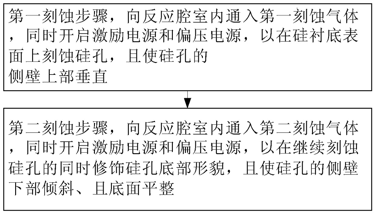
[0028] In order to enable those skilled in the art to better understand the technical solution of the present invention, the deep silicon hole etching method provided by the present invention will be described in detail below in conjunction with the accompanying drawings.

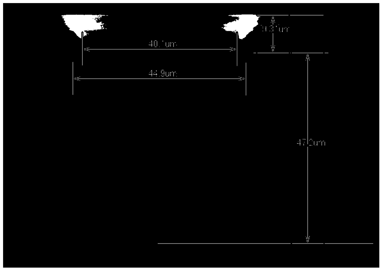
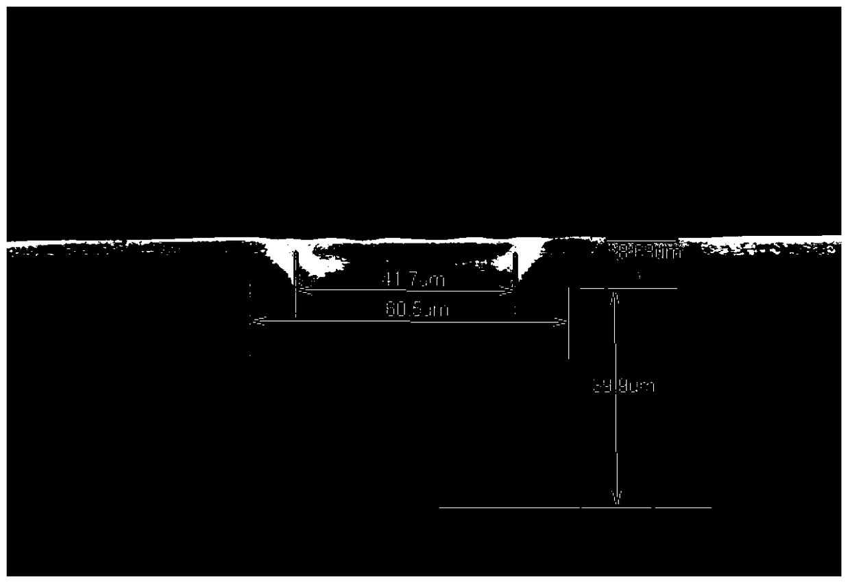
[0029] The deep silicon hole etching method is to etch a deep hole with a relatively high aspect ratio on a silicon substrate, and an inductively coupled plasma (Inductively Coupled Plasma, hereinafter referred to as ICP) equipment is usually used to perform the above etching process. Specifically, the etching gas is fed into the reaction chamber, and the excitation power supply and the bias power supply are turned on at the same time. The excitation power supply is used to apply excitation power to the reaction chamber, so that the etching gas in the reaction chamber is excited to form plasma; the bias voltage The power supply is used to apply bias power to the silicon substrate, so that the plasma etches t...


PUM


Abstract

The invention provides a deep silicon hole etching method, comprising a first etching step of inletting a first etching gas into a reaction chamber, and meanwhile switching on an excitation power supply and a bias power supply so as to etch a silicon hole in a silicon substrate, the first etching gas including a mixed gas of SF6 and O2, the gas flows of which are set to enable a vertical upper portion for the side wall of the silicon wall; and a second etching step of inletting a second etching gas into the reaction chamber, and meanwhile switching on the excitation power supply and the bias power supply so as to modify the morphology of the bottom of the silicon hole while continuing the etching of the silicon hole, the second etching gas including a mixed gas of SF6, C4F8, He and O2, the gas flows of which are set to enable the bottom width of the side wall of the silicon wall to shrink and the bottom of the silicon hole to be smooth. The invention can be used for obtaining a deep silicon hole of which the upper portion of the side wall is vertical, the bottom width of the side wall shrinks and the bottom is flat and smooth.

Description

technical field [0001] The invention relates to the technical field of microelectronics, in particular to a deep silicon hole etching method. Background technique [0002] As MEMS devices and MEMS systems are more and more widely used in the fields of automobiles and consumer electronics, the dry plasma deep silicon etching process has gradually become one of the hottest processes in the field of MEMS processing. [0003] An existing silicon deep hole etching method is to use SF 6 、C 4 f 8 and O 2 The mixed gas is used as an etching gas to etch deep silicon holes in a single step on a silicon wafer. Its main features are: by adjusting SF 6 Different flow rates and bias powers were used to obtain different sidewall morphologies. Among them, the higher SF 6 The higher the flow rate, the larger the silicon hole depth can be obtained, and the more inclined side wall morphology can be obtained by using lower bias power. Typical process parameters are: chamber pressure 90m...

Claims


Application Information

Patent Timeline
Patent Type & Authority Patents(China)
IPC IPC(8): H01L21/768H01L21/3065
Inventor 李战强蒋中伟
Owner BEIJING NAURA MICROELECTRONICS EQUIP CO LTD
Why Eureka
Try Eureka