
A Soi MOS Tube Dose Rate Radiation SPICE Macro Model Modeling Method

A technology of dose rate and macro model, applied in instrumentation, calculation, electrical and digital data processing, etc., can solve problems such as sag and peak current sag, and achieve the effect of improving simulation accuracy, efficiency and modeling accuracy.

Inactive Publication Date: 2019-10-08
INST OF ELECTRONICS ENG CHINA ACAD OF ENG PHYSICS
View PDF4 Cites 0 Cited by
  • Summary
  • Abstract
  • Description
  • Claims
  • Application Information

AI Technical Summary

Problems solved by technology

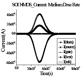
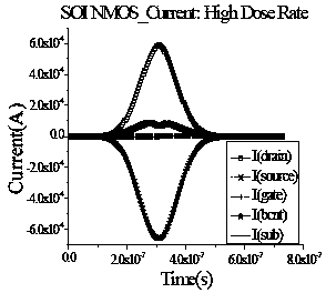
However, if Figure 1-2 As shown, we found that when the dose rate of radiation increases to a certain level, the peak current at the source terminal no longer increases proportionally, but a significant depression phenomenon appears, which cannot be explained by Honeywell's parasitic diode model of
In fact, this is mainly caused by the parasitic triode (BJT) in the device. When the high dose rate is irradiated, the microscopic potential changes in different regions inside the device cause the parasitic BJT to turn on, and the source starts to collect holes, so the source A negative current is superimposed on it, causing its peak current to sag

Method used


Image

  • A Soi MOS Tube Dose Rate Radiation SPICE Macro Model Modeling Method
  • A Soi MOS Tube Dose Rate Radiation SPICE Macro Model Modeling Method
  • A Soi MOS Tube Dose Rate Radiation SPICE Macro Model Modeling Method

Examples


Embodiment Construction

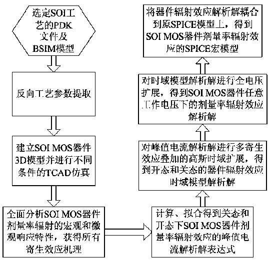
[0030] The method of the invention is suitable for MOS devices of deep submicron SOI technology, mainly including SOI technology of 0.5um, 0.35um, 0.18um, 0.15um, 0.13um and other sizes. Take the 0.5um process as an example below, combined with image 3 The flow chart shown illustrates the specific implementation process of the present invention.

[0031] First select a 0.5um SOI process line of a process manufacturer and obtain its PDK file and BSIM model, and then use Hspice (a circuit SPICE model simulator under the American Synopsys company) to simulate and obtain the parameters used for reverse process parameter extraction. standard control I D -V G curve. Then based on the known device structure, some existing process parameters (such as substrate thickness, silicon film thickness, buried oxide layer thickness, substrate uniform doping concentration, N / P well region doping depth, etc.) and various unknown parameters Establish a 3D model of the SOI MOS device and perf...


PUM


Abstract

The invention relates to a SPICE (Simulation Program for Integrated Circuit Emphasis) macro model molding method for SOIMOS (Silicon on Insulator Metal Oxide Semiconductor) transistor dose rate radiation. The method mainly comprises the following steps: coupling radiation response features of a device under different conditions to an original SPICE model under a non-radiation condition of the device through a macro model technology specific to a dose rate radiation effect of an SOI MOS device in order to form a basic device unit model including radiation responses; and predicting a radiation response feature of a whole integrated circuit by direct calling of the unit model and system simulation. Through adoption of the method, functions and performance of the designed integrated circuit under specific radiation conditions can be effectively simulated; a reference basis is provided for an anti-radiation SoC (System on Chip) design; the tape-out times are reduced; the cost is lowered greatly; the development period is accelerated; and the efficiency is increased.

Description

technical field [0001] The invention designs a method for establishing a SPICE macro model of the radiation effect of a device, and in particular relates to a method for modeling a SPICE macro model of the dose rate radiation of an SOI MOS tube. Background technique [0002] The silicon on insulator (Silicon On Insulator, SOI) process refers to introducing a buried oxide layer (silicon dioxide) into the substrate of traditional bulk silicon, so as to achieve the effect of full dielectric isolation of the device. Because the SOI process can eliminate the parasitic latch-up effect of the bulk silicon CMOS circuit, and has strong resistance to single event and dose rate radiation, it has received more and more attention in the field of radiation resistance. SPICE (Simulation Program for Integrated CircuitEmphasis) is the most commonly used circuit-level simulation program in the device design industry. Various software manufacturers provide different versions of SPICE software ...

Claims


Application Information

Patent Timeline
Patent Type & Authority Patents(China)
IPC IPC(8): G06F17/50
CPCG06F30/367
Inventor 梁堃李顺解磊孙鹏代刚李沫
Owner INST OF ELECTRONICS ENG CHINA ACAD OF ENG PHYSICS
Learn More