Nitride epitaxial growth method

A technology of epitaxial growth and nitride, applied in the field of semiconductor, to achieve the effect of low dislocation density, high crystal quality and lower dislocation density

Active Publication Date: 2016-07-13
SHANGHAI SIMGUI TECH
View PDF3 Cites 5 Cited by
  • Summary
  • Abstract
  • Description
  • Claims
  • Application Information

AI Technical Summary

Problems solved by technology

[0005] The technical problem to be solved by the present invention is to provide a nitride epitaxial growth method, which can alleviate the problems of lattice mismatch and thermal mismatch in growing nitride heteroepitaxial growth, reduce stress, and reduce dislocation density.

Method used


Image

  • Nitride epitaxial growth method
  • Nitride epitaxial growth method
  • Nitride epitaxial growth method

Examples


Embodiment Construction

[0020] The specific implementation of a nitride epitaxial growth method provided by the present invention will be described in detail below with reference to the accompanying drawings.

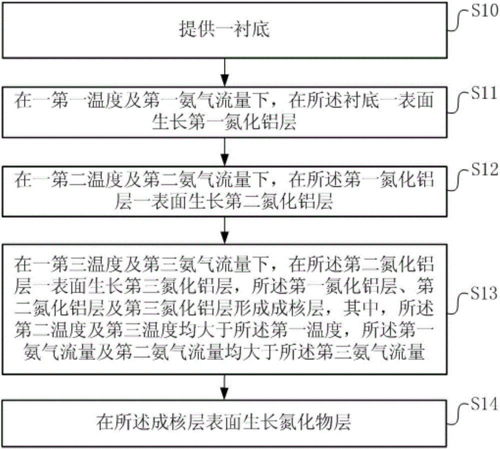
[0021] see figure 1 , a nitride epitaxial growth method of the present invention comprises the following steps: step S10, providing a substrate; step S11, growing first nitrogen on a surface of the substrate at a first temperature and a first ammonia flow rate Aluminum layer; step S12, at a second temperature and a second ammonia gas flow, grow a second aluminum nitride layer on a surface of the first aluminum nitride layer; step S13, at a third temperature and a third Under the flow of ammonia gas, a third aluminum nitride layer is grown on the surface of the second aluminum nitride layer, and the first aluminum nitride layer, the second aluminum nitride layer and the third aluminum nitride layer form a nucleation layer , wherein, the second temperature and the third temperature are greater ...


PUM

PropertyMeasurementUnit
thicknessaaaaaaaaaa
thicknessaaaaaaaaaa
thicknessaaaaaaaaaa

Abstract

The invention provides a nitride epitaxial growth method comprising the following steps that a substrate is provided; a first aluminum nitride layer is grown on one surface of the substrate under first temperature and first ammonia gas flow; a second aluminum nitride layer is grown on one surface of the first aluminum nitride layer under second temperature and second ammonia gas flow; a third aluminum nitride layer is grown on one surface of the second aluminum nitride layer under third temperature and third ammonia gas flow, and a nucleation layer is formed by the first aluminum nitride layer, the second aluminum nitride layer and the third aluminum nitride layer, wherein second temperature and third temperature are greater than first temperature, and the first ammonia gas flow and the second ammonia gas flow are greater than the third ammonia gas flow; and a nitride layer is grown on the surface of the nucleation layer. The advantages of the nitride epitaxial growth method are that problems of crystal lattice mismatch and thermal mismatch existing in nitride heteroepitaxy growth can be alleviated, stress can be reduced and dislocation density can be reduced.

Description

technical field [0001] The invention relates to the technical field of semiconductors, in particular to a nitride epitaxial growth method. Background technique [0002] GaN-based semiconductor materials have excellent and unique electrical and optical properties, such as wide direct bandgap, high thermal conductivity, large breakdown electric field strength, high temperature and high pressure resistance, corrosion resistance, radiation resistance, etc., suitable for applications in harsh conditions Environment. Gallium nitride-based semiconductor materials can be used to prepare optoelectronic devices such as ultraviolet / blue / green light-emitting diodes (LEDs), lasers (LDs), photodetectors, and high-frequency, high-voltage, high-power, radiation-resistant high electron mobility transistors (HEMTs) ) and power electronics (power) devices and other electronic devices. [0003] At present, the single crystal substrate preparation technology of gallium nitride or aluminum nitr...

Claims


Application Information

Patent Timeline
Patent Type & Authority Applications(China)
IPC IPC(8): H01L21/02C30B25/16C30B29/40
CPCC30B25/16C30B29/403H01L21/02458H01L21/0254H01L21/0262
Inventor 闫发旺张峰赵倍吉谢杰
Owner SHANGHAI SIMGUI TECH
Why Eureka
Try Eureka