Semiconductor structure and forming method therefor

A semiconductor and isolation structure technology, which is applied in the field of semiconductor structure and its formation, can solve the problems of semiconductor device electrical performance degradation, etc., and achieve the effects of improving electrical performance, optimizing electrical isolation effect, and increasing breakdown voltage

Active Publication Date: 2016-07-13
SHANGHAI HUAHONG GRACE SEMICON MFG CORP
View PDF3 Cites 1 Cited by
  • Summary
  • Abstract
  • Description
  • Claims
  • Application Information

AI Technical Summary

Problems solved by technology

[0003] However, the well isolation structure in the prior art is likely to ca

Method used


Image

  • Semiconductor structure and forming method therefor
  • Semiconductor structure and forming method therefor
  • Semiconductor structure and forming method therefor

Examples


Embodiment Construction

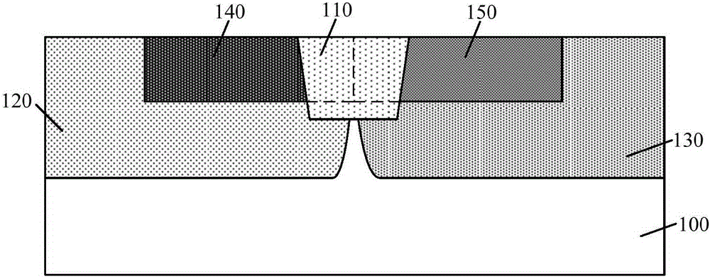
[0020] It can be seen from the background art that the well isolation structure in the prior art is likely to cause the degradation of the electrical performance of the semiconductor device. Analyze the reasons for this:

[0021] Such as figure 1 As shown, the structure of an embodiment of the well isolation structure includes: a substrate 100; an adjacent N well (Nwell) 120 and a P well (Pwell) 130 located in the substrate 100; the N well 120 and the P well An isolation structure 110 (such as ShallowTrenchIsolation, STI) is formed between 130, and the isolation structure 110 is a well isolation structure between the adjacent N well 120 and P well 130; the N well 120 is close to the isolation structure. An N-type heavily doped region 140 is formed on one side of the structure 110 for forming an N-type device; a P-type heavily doped region 150 is formed in the P well 130 near the side of the isolation structure 110 for forming a P-type device. Through the well isolation stru...


PUM


Abstract

The invention discloses a semiconductor structure and a forming method therefor. The method comprises the steps: providing a substrate; forming an isolation structure on the substrate, wherein the isolation structure is used for dividing the substrate into a first region and a second region; forming a first well region in the first region of the substrate; forming a second well region in the second region of the substrate, wherein the doping type of the second well region is different from the doping type of the first well region; forming a pseudo grid structure located on the isolation structure; taking the pseudo grid structure as a mask, and forming a second heavily-doped region in the second well region, wherein the doping type of the second heavily-doped region is the same as the doping type of the second well region; taking the pseudo grid structure as the mask, and forming a first heavily-doped region in the first well region, wherein the doping type of the first heavily-doped region is the same as the doping type of the first well region. The method forms the pseudo grid structure on the isolation structure at the junction of the first and second regions, and the pseudo grid structure can serve as an ion injection mask during the forming of the doped regions, thereby preventing doping ions in the heavily-doped regions from entering the adjacent well region or heavily-doped region, and improving the breakdown voltage of an adjacent device.

Description

technical field [0001] The invention relates to the field of semiconductors, in particular to a semiconductor structure and a forming method thereof. Background technique [0002] In the manufacturing process of semiconductor devices, Shallow Trench Isolation (STI) or Local Oxidation of Silicon (LOCOS) is often used as the well isolation structure between the P well (Pwell) and the N well (Nwell). to achieve device isolation. Two adjacent well regions are formed in the substrate, a heavily doped region is also formed in the corresponding well regions, an isolation structure is formed between the adjacent well regions, and the depth of the adjacent well regions is greater than the isolation structure depth. Through the well isolation structure, the punch-through of adjacent devices can be suppressed, and the leakage of devices can be reduced. [0003] However, the well isolation structure in the prior art tends to cause the degradation of electrical performance of the semi...

Claims


Application Information

Patent Timeline
IPC IPC(8): H01L21/762H01L27/088H01L21/8232
CPCH01L21/762H01L21/8232H01L27/088
Inventor 王卉曹子贵康军刘宇
Owner SHANGHAI HUAHONG GRACE SEMICON MFG CORP
Why Eureka
Try Eureka