Graphene field effect transistor and manufacturing method thereof

A technology of field effect transistors and manufacturing methods, applied in semiconductor/solid-state device manufacturing, semiconductor devices, electrical components, etc., to achieve the effects of simple process flow, increased on-state current, and increased conductive channels

Active Publication Date: 2016-07-13
INST OF MICROELECTRONICS CHINESE ACAD OF SCI
View PDF5 Cites 7 Cited by
  • Summary
  • Abstract
  • Description
  • Claims
  • Application Information

AI Technical Summary

Problems solved by technology

Currently, the current cut-off frequency f of the graphene field effect transistor T Although it has reached 427GHz, it is still far below its ideal value

Method used


Image

  • Graphene field effect transistor and manufacturing method thereof
  • Graphene field effect transistor and manufacturing method thereof
  • Graphene field effect transistor and manufacturing method thereof

Examples


Embodiment Construction

[0032] In order to make the object, technical solution and advantages of the present invention clearer, the present invention will be further described in detail below in conjunction with specific embodiments and with reference to the accompanying drawings.

[0033] The invention discloses a method for manufacturing a graphene field effect transistor, comprising the following steps:

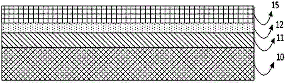
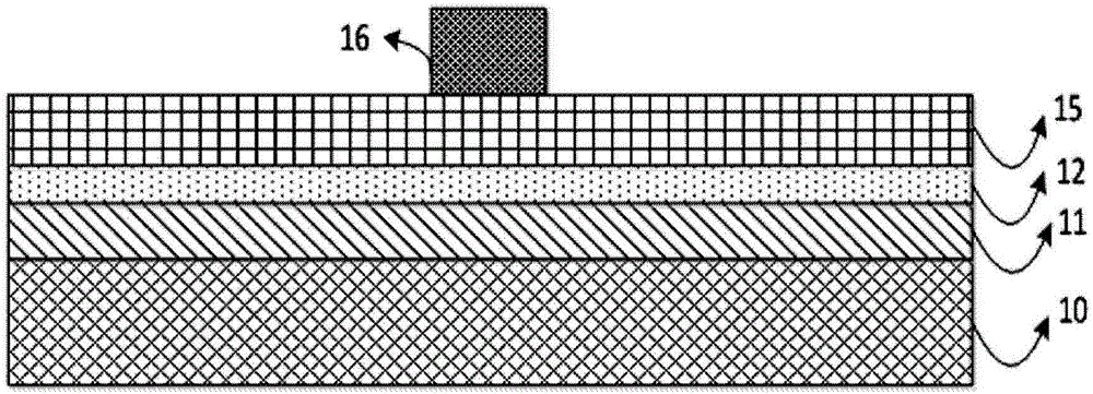
[0034] sequentially forming a graphene layer, a gate dielectric layer and a top gate metal electrode layer on the substrate;

[0035] Using the top gate metal electrode layer as a mask, etch the upper surface of the device formed above to remove the gate dielectric layer outside the area covered by the top gate metal electrode layer;

[0036] Continue to use the top gate metal electrode layer as a mask to etch the graphene layer in the channel region, destroying the lattice structure of the graphene material in the graphene layer to form defects;

[0037] Forming a metal thin film layer on the d...


PUM


Abstract

Provided are a graphene field effect transistor and a manufacturing method thereof.The manufacturing method comprises the following steps that a top gate metal is used as a gate medium under a mask protecting top gate metal, and a gate medium layer is etched to remove the gate medium covering a graphene active area between a gate source and a gate drain; a top gate electrode is used as a mask to etch graphene, and a lattice structure of a graphene material is destroyed to form a defect; then, a metal film layer is formed on a formed device, and a source electrode and a drain electrode are prepared on the metal film layer; and the completed device is annealed.By the adoption of the manufacturing method, the separation distance between the gate source and the gate drain can be decreased, the graphene pollution caused by a device machining process is effectively avoided, the lower contact resistivity can be obtained by partially etching the graphene material in a contact area, and accordingly the performance of the graphene transistor can be improved.

Description

technical field [0001] The invention belongs to the field of field-effect transistor manufacturing, and in particular relates to a graphene field-effect transistor and a manufacturing method thereof. Background technique [0002] Due to the ultrahigh carrier mobility and saturation drift velocity, graphene has attracted extensive attention in recent years and is expected to be applied in the future high-speed electronics and radio frequency fields. Currently, the current cut-off frequency f of the graphene field effect transistor T Although it has reached 427GHz, it is still far less than its ideal value. One of the important factors is excessive parasitic resistance. The influence of contact area resistance and access area resistance on the frequency characteristics of graphene devices becomes more obvious as the gate length decreases. Therefore, reducing the contact resistance and the resistance of the access area is the key to improving its radio frequency performance....

Claims


Application Information

Patent Timeline
Patent Type & Authority Applications(China)
IPC IPC(8): H01L29/78H01L21/336H01L21/28H01L29/10H01L29/16
CPCH01L21/28H01L29/1033H01L29/1606H01L29/66477H01L29/78
Inventor 金智王少青毛达诚史敬元彭松昂张大勇
Owner INST OF MICROELECTRONICS CHINESE ACAD OF SCI
Why Eureka
Try Eureka