Band-gap reference voltage source without resistor or operational amplifier

A reference voltage source, no op amp technology, applied in the direction of adjusting electrical variables, control/regulating systems, instruments, etc., can solve problems such as large area and complex structure, and achieve a layout area, simple circuit structure, and simple circuit structure. Effect

Inactive Publication Date: 2016-07-20
JIANGNAN UNIV
View PDF0 Cites 22 Cited by
  • Summary
  • Abstract
  • Description
  • Claims
  • Application Information

AI Technical Summary

Problems solved by technology

[0003] The purpose of the present invention is to provide a low-voltage, small-area, low-power bandgap reference voltage source circuit to solve the existing problems of large area and complex structure

Method used


Image

  • Band-gap reference voltage source without resistor or operational amplifier
  • Band-gap reference voltage source without resistor or operational amplifier

Examples


Embodiment Construction

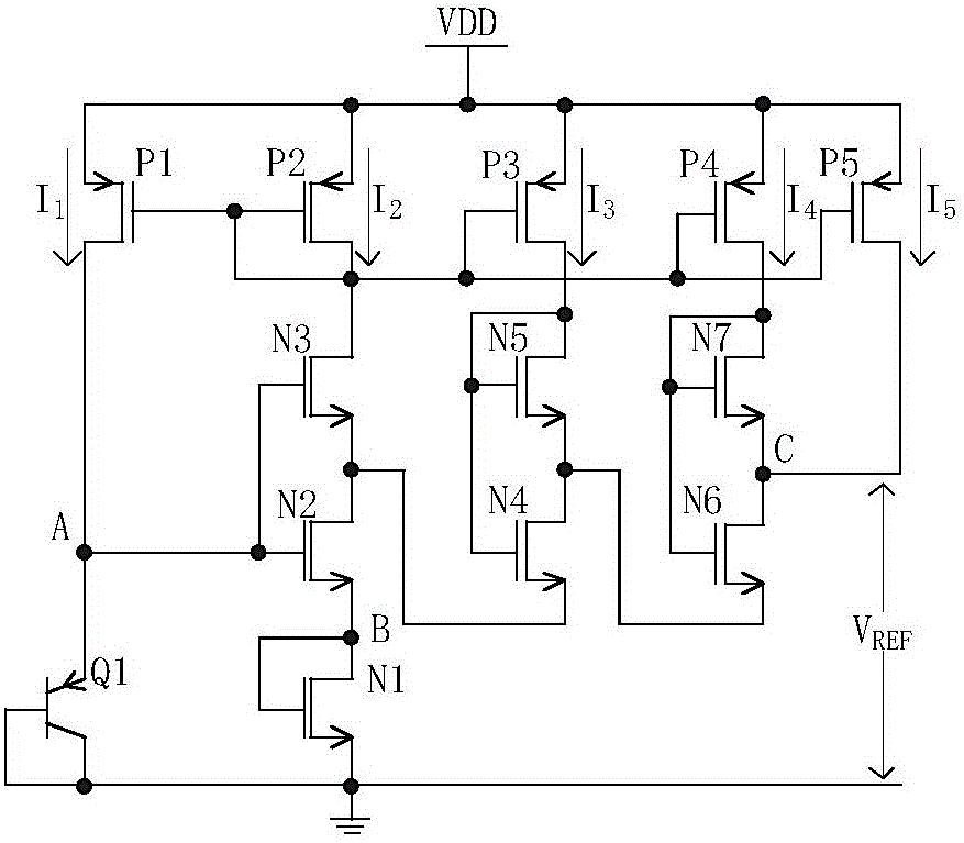
[0011] like figure 1 As shown, a resistance-free and no-op-amp bandgap reference voltage source circuit according to the present invention is described. Including the first PMOS transistor P1, the second PMOS transistor P2, the third PMOS transistor P3, the fourth PMOS transistor P4, the fifth PMOS transistor P5, the first NMOS transistor N1, the second NMOS transistor N2, the third NMOS transistor N3, the Four NMOS transistors N4, fifth NMOS transistor N5, sixth NMOS transistor N6, seventh NMOS transistor N7 and first BJT transistor Q1. The gate of the first PMOS transistor P1 is respectively connected to the gate of the second PMOS transistor P2, the drain of the second PMOS transistor P2, the gate of the third PMOS transistor P3, the gate of the fourth PMOS transistor P4 and the fifth The gate of the PMOS transistor P5; the drain of the first PMOS transistor P1 is respectively connected to the emitter of the first BJT transistor Q1, the gate of the second NMOS transistor N...


PUM


Abstract

The invention relates to a band-gap reference voltage source circuit without a resistor structure or an operational amplifier structure. The band-gap reference voltage source circuit comprises BJTs and MOS tubes. PN junction voltage of the BJTs has a negative temperature coefficient feature, and the source-drain terminal voltage of the MOS tubes is in a direct proportion relation along with the temperature and is positive temperature coefficient voltage. The PN junction voltage is scaled down and is added with the source-drain terminal voltage according to different weights, and thus a reference output voltage which does not change along with temperatures is obtained. According to the band-gap reference voltage source circuit, an operational amplifier and resistor network in a traditional band-gap reference voltage source circuit is omitted, low voltage and a small layout area are achieved, the MOS tubes in a sub-threshold state have small drain current, and thus low power consumption is achieved. The band-gap reference voltage source circuit has the advantages of being high in precision, simple in structure and high in practicability.

Description

technical field [0001] The invention belongs to the field of integrated circuits, and in particular relates to a bandgap reference voltage source circuit. Background technique [0002] In the traditional bandgap reference voltage source circuit, its core structure is composed of BJT tube, operational amplifier and resistor network. In order to obtain a high-performance bandgap reference voltage in traditional circuits, high-performance operational amplifiers and precisely matched resistor networks are required in circuit design, which not only increases the design workload, but also increases the complexity of circuit design. The amplifier structure occupies a large chip area and increases the design cost; at the same time, the minimum operating voltage of the operational amplifier limits the minimum input voltage of the bandgap reference circuit. In order to obtain a bandgap voltage reference circuit with low voltage, small area and low power consumption, a new bandgap vol...

Claims


Application Information

Patent Timeline
Patent Type & Authority Applications(China)
IPC IPC(8): G05F3/26
CPCG05F3/267
Inventor 王利王闪屠思远汪海盛炜梁钰
Owner JIANGNAN UNIV
Why Eureka
Try Eureka