

Shifting register and light-emitting control circuit
A shift register, capacitor technology, applied in static memory, digital memory information, instruments, etc., can solve the problems of signal line crosstalk, adverse effects on stability and reliability, clock signal multiplication, etc.
- Summary
- Abstract
- Description
- Claims
- Application Information
AI Technical Summary
Problems solved by technology
Method used
Image

Examples
Embodiment 1
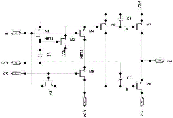
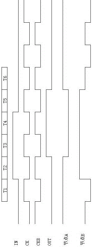
[0044] Please refer to figure 1 , in a preferred embodiment of the present invention, the shift register unit circuit includes two input clock ports (including the first clock signal CK, the second clock signal CKB), a signal input terminal IN, an output port OUT and a constant voltage Signal VGH (high level), VGL (low level). The schematic diagram of the shift register circuit is as follows figure 1 shown.
[0045] The schematic diagram consists of 8 P-channel thin film transistors (M1~M8) and 3 capacitors (C1~C3). For the sake of simplicity in the schematic diagram, all nodes with the same name in the diagram are connected together even if there is no direct connection. The schematic structure is described as follows:
[0046] The gate of the first thin film transistor is connected to the signal input terminal IN, the first source / drain is connected to VGH, and the second source / drain is connected to the NET1 node;
[0047] The gate of the second thin film transistor is...
Embodiment 2
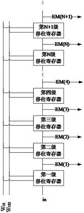
[0068] Please refer to image 3 A lighting control circuit comprising a plurality of shift registers connected in cascade. The cascaded circuit such as image 3 As shown, the shift register units at all levels are consistent. Specifically, the output port of the previous stage is connected to the input port of the subsequent stage, and EM(N) is the output signal of the Nth stage, and also serves as the input signal of the N+1th stage. The input clock port connections are different for each stage. The connection of the three input clock ports of each stage is described as follows: the first clock signal of the first stage is connected to CK, the second clock signal is connected to CKB; the first clock signal of the second stage is connected to CKB, the second clock signal is connected to CK, and the third The connection method of the first level is the same as that of the first level, and the connection method of the fourth level is the same as that of the second level, and ...
PUM
 Abstract
Description
Claims
Application Information