Method and system for realizing p-type nitride enhanced hemt through in-situ etch monitoring

An in-situ etching and nitride technology, which is applied in the direction of electrical components, semiconductor/solid-state device manufacturing, semiconductor/solid-state device testing/measurement, etc., to achieve the effect of avoiding over-etching, avoiding incomplete etching, and low cost

Active Publication Date: 2018-06-22
SUZHOU NENGWU ELECTRONICS TECH
View PDF5 Cites 1 Cited by
  • Summary
  • Abstract
  • Description
  • Claims
  • Application Information

AI Technical Summary

Problems solved by technology

[0004] The main purpose of the present invention is to provide a method, system and application thereof for monitoring in-situ etching of P-type semiconductor HEMT devices, especially a method and system for developing precise and complex etching processes, so as to overcome the shortcomings of the prior art insufficient

Method used


Image

  • Method and system for realizing p-type nitride enhanced hemt through in-situ etch monitoring
  • Method and system for realizing p-type nitride enhanced hemt through in-situ etch monitoring
  • Method and system for realizing p-type nitride enhanced hemt through in-situ etch monitoring

Examples


Embodiment Construction

[0025] The technical solutions of the present invention will be explained in more detail below. However, it should be understood that within the scope of the present invention, the above-mentioned technical features of the present invention and the technical features specifically described in the following (eg, the embodiments) can be combined with each other to form new or preferred technical solutions. Due to space limitations, it is not repeated here.

[0026] An embodiment of the present invention provides a method for realizing a P-type nitride-enhanced HEMT by monitoring in-situ etching, which includes:

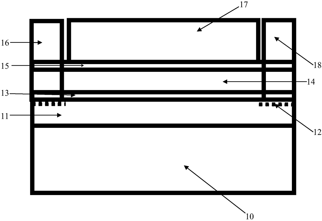
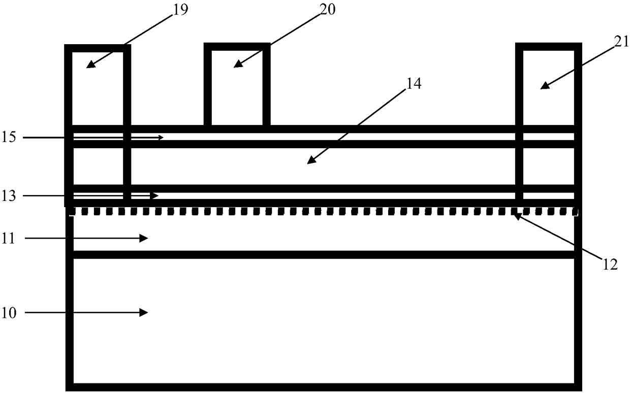
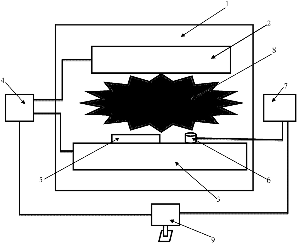
[0027] Place the etched sample and the counterplate at the equivalent etching position in the etching equipment to ensure that the etched sample and the counterplate are under the same etching conditions, and the counterplate has the same epitaxy as the etched sample structure, and the co-plate has two electrodes, and the two electrodes are electrically connected by tw...


PUM


Abstract

The invention discloses a method and a system for realizing a P-type nitride enhanced HEMT (High Electron Mobility Transistor) through in-situ etching monitoring. In one typical embodiment, through directly exposing an etching surface of an etching sample in a plasma and placing a test wafer plated with electrodes in an etching position equivalent to a sample in etching equipment, the etching rate on the sample is equal to that on the test wafer, so that an etching condition of a P-type semiconductor on the sample can be monitored through the change of the current between two electrodes on the test wafer, and then the obtained current signal is input into a computer and the computer controls the etching condition to realize a controllable and precise etching technology with feedback. According to the method and the system, the defects caused by realizing different etching depths through the single etching condition, the single etching rate and the etching time simply in the existing etching technology are effectively solved, and preparation of the P-type cap layer enhanced HEMT device can be realized at high precision and high repeatability.

Description

technical field [0001] The invention relates to a method and a system for developing precise and complex etching processes, in particular to a method and system for realizing a P-type nitride enhanced HEMT by monitoring in-situ etching. Background technique [0002] When the existing III-nitride semiconductor HEMT devices are used as high-frequency devices or high-voltage and high-power switching devices, especially as power switching devices, the enhancement mode HEMT device is helpful to improve the safety of the system compared with the depletion mode HEMT device. performance, reduce the loss of the device and simplify the design circuit. At present, the main methods for realizing enhanced HEMT include thin barrier layers, recessed gate structures, P-type capping layers, and F processing techniques. But each technology has its own shortcomings. For example, the world's first enhancement-mode HEMT device is implemented with a thinner barrier layer. This method does not u...

Claims


Application Information

Patent Timeline
Patent Type & Authority Patents(China)
IPC IPC(8): H01L21/66H01L21/67
CPCH01L21/67253H01L22/14H01L22/26
Inventor 张志利张宝顺蔡勇付凯于国浩孙世闯宋亮李维毅
Owner SUZHOU NENGWU ELECTRONICS TECH
Why Eureka
Try Eureka