Sub-micron scale glass subsurface defect detection device and method
A technology for subsurface defects and detection devices, which is used in measurement devices, instruments, scientific instruments, etc., can solve the problems of inability to obtain extended depth, inability to obtain local data, and high requirements for mechanical devices, and achieve detection sensitivity and signal-to-noise ratio. High detection sensitivity and signal-to-noise ratio, ensuring the effect of stability
- Summary
- Abstract
- Description
- Claims
- Application Information
AI Technical Summary
Problems solved by technology
Method used
Image

Examples
Embodiment 1
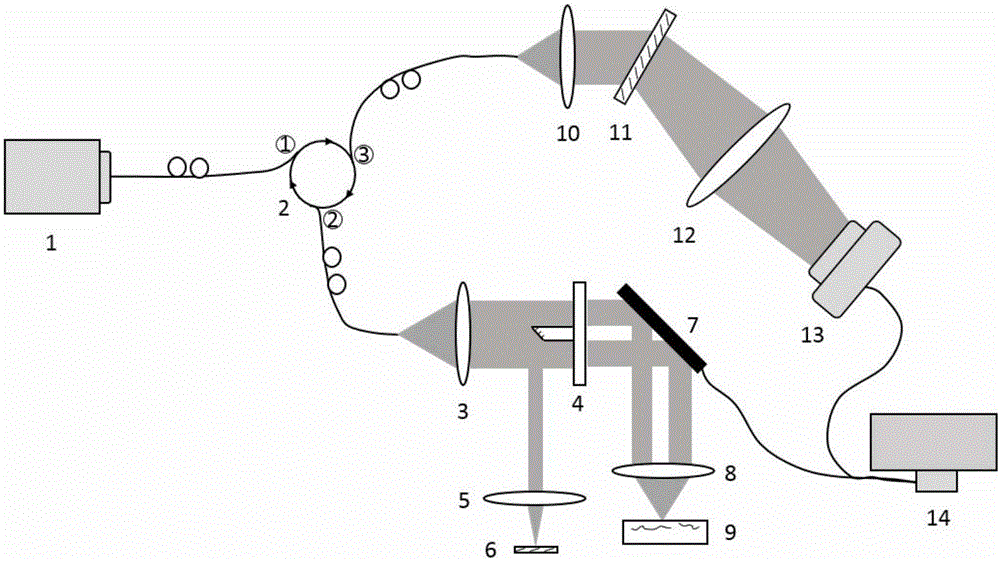
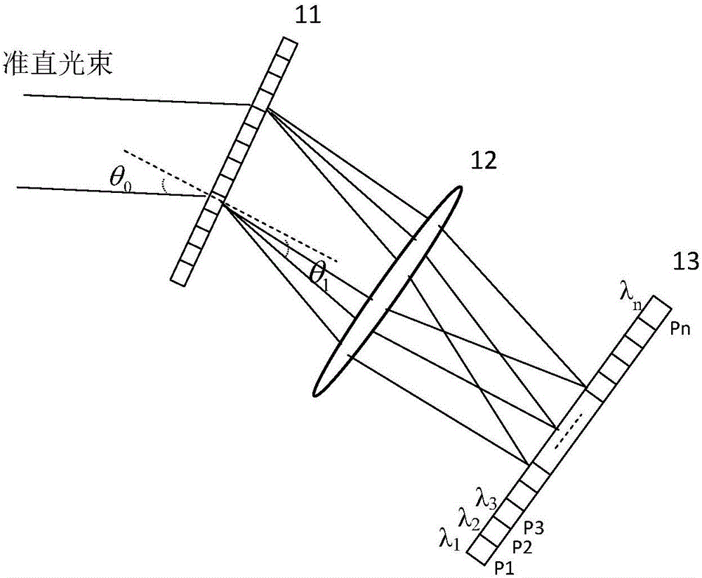
[0049] The supercontinuum light source 1 described in this embodiment uses SC480 from Fianium Company of the United Kingdom. The total output power of the laser is about 2w, and the wavelength bandwidth is about 2000nm, and the maximum wavelength is 2400nm. The 45° cylindrical reflector 4 selects NT54-092 from Edmund Optics Company, and its cylindrical surface diameter is 2 mm. Both the reference objective lens 5 and the sample objective lens 8 are achromatic lenses with a focal length of 10 mm and a numerical aperture of 0.4 from Thorlabs. The two-dimensional scanning galvanometer 7 is GVS012 with a clear aperture of 10 mm from Thorlabs. The test piece 9 is glass with submicron cracks on the subsurface. The transmission grating 11 is 1002-1 from Wasatch Company, the number of line pairs is 1200, and the working wavelength is 830nm. The focusing lens 12 is a two-inch achromatic lens from Thorlabs. The photodetector 13 is a linear array EM2 from E2V Company.
[0050] The su...
PUM
| Property | Measurement | Unit |
|---|---|---|
| Wavelength | aaaaa | aaaaa |
| Bandwidth | aaaaa | aaaaa |
| Center wavelength | aaaaa | aaaaa |
Abstract
Description
Claims
Application Information