Mosfet packaging structure and its manufacturing method

A technology of packaging structure and conductive pad, which is used in semiconductor/solid-state device manufacturing, semiconductor/solid-state device components, semiconductor devices, etc. The effect of high production efficiency, shortened interconnection distance and excellent heat dissipation performance

Active Publication Date: 2019-03-26
HUATIAN TECH KUNSHAN ELECTRONICS
View PDF7 Cites 1 Cited by
  • Summary
  • Abstract
  • Description
  • Claims
  • Application Information

AI Technical Summary

Problems solved by technology

The back gold process of this packaging solution is complicated, the yield rate is low, and the cost of using through-silicon via (TSV) technology is high

Method used


Image

  • Mosfet packaging structure and its manufacturing method
  • Mosfet packaging structure and its manufacturing method
  • Mosfet packaging structure and its manufacturing method

Examples


Embodiment approach

[0052] As a preferred embodiment, a method for manufacturing a MOSFET packaging structure of the present invention includes the following steps:

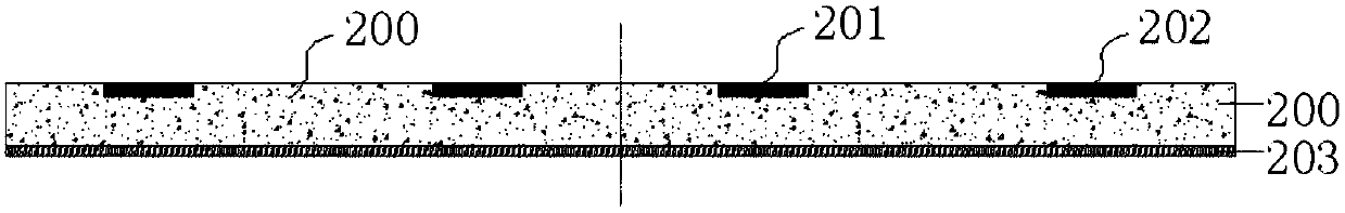
[0053] a. see figure 1 , providing several MOSFET chips 200, the front side of the MOSFET chip includes a source conductive pad 201 and a gate conductive pad 202, and the back side of the MOSFET chip includes a drain region and a metal layer 203 on the drain region, wherein the The gate conductive pad is insulated from the source conductive pad and the drain region;

[0054] During specific implementation, a plurality of MOSFET chips can be cut and separated from a MOSFET wafer.

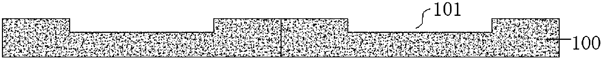
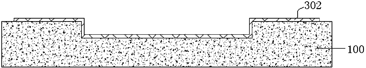
[0055] b. see figure 2 , image 3 and Figure 4 , providing a silicon wafer with a plurality of sunken grooves 101 on the surface, as a silicon substrate 100, plating a conductive layer on the surface of the silicon wafer with sunken grooves, the conductive layer covers the bottom of the sunken grooves, and extends to the surface of the silicon wafer,...


PUM


Abstract

The invention discloses a MOSFET packaging structure and a manufacturing method thereof. The packaging structure includes a silicon substrate and a MOSFET chip. The front side of the MOSFET chip includes a source conductive pad and a gate conductive pad, and the back side includes a drain region and a metal layer. There is a sinking groove on the surface of the substrate, and the bottom of the sinking groove is laid with a conductive layer extending to the surface of the substrate as a drain conductive pad. The back of the MOSFET chip is mounted on the bottom of the sinking groove, and the metal layer and the sinking groove The conductive layer at the bottom is connected by metal bonding, the conductors interconnected with the outside are formed on the source conductive pad, the gate conductive pad and the drain conductive pad, and the part other than the conductor on the front side of the silicon substrate is encapsulated by the protective layer. The present invention guides the drain current on the back of the MOSFET with a vertical structure to the front of the MOSFET, realizes that the source, gate, and drain are electrically on the same side for wafer-level packaging, and the large-area conductive layer ensures a good chip Heat dissipation effect; avoiding the TSV process through silicon vias, simplifying the process steps and reducing the packaging cost.

Description

technical field [0001] The invention belongs to the technical field of semiconductor packaging, and in particular relates to a MOSFET packaging structure and a manufacturing method thereof. Background technique [0002] MOSFET (Metal Oxide Semiconductor Field Effect Transistor) is a field effect transistor that uses electric field effects to control semiconductors. Due to the characteristic of realizing low power consumption voltage control, MOSFET has been widely used in a large number of electronic devices in recent years, including power supplies, automotive electronics, computers and smart phones, and has received more and more attention. [0003] A MOSFET device operates by applying an appropriate voltage to the gate of the MOSFET device, which turns on the device and forms a channel connecting the source and drain of the MOSFET to allow current to flow. In a MOSFET device, it is desirable to have a low drain-on-source resistance, RDS(on), when the transistor is on. T...

Claims


Application Information

Patent Timeline
Patent Type & Authority Patents(China)
IPC IPC(8): H01L23/498H01L23/482H01L21/60
CPCH01L23/49844H01L24/73H01L24/92H01L24/97H01L2224/73267H01L2224/9201H01L2224/92144H01L2224/04105H01L2224/06181H01L2224/12105H01L2224/19H01L2224/32225H01L2224/32245H01L2224/92244H01L2924/15153
Inventor 于大全肖智轶崔志勇耿增华
Owner HUATIAN TECH KUNSHAN ELECTRONICS
Why Eureka
Try Eureka