
Silicon carbide BJT (bipolar junction transistor)

A bipolar junction and transistor technology, applied in the direction of transistors, semiconductor devices, electrical components, etc., to achieve the effect of reducing electron concentration, reducing the probability of contact, and reducing the recombination current

Inactive Publication Date: 2016-08-17
UNIV OF ELECTRONICS SCI & TECH OF CHINA
View PDF4 Cites 3 Cited by
  • Summary
  • Abstract
  • Description
  • Claims
  • Application Information

AI Technical Summary

Problems solved by technology

Although this structure reduces the recombination current and improves the current gain, it still does not fundamentally solve the problem of SiC / SiO2 high interface state; and the metal on the SiO2 dielectric layer is an electrode that needs to be applied voltage, which leads to the failure of this structure. The device is a four-terminal device. For triodes, four-terminal devices have many disadvantages compared with three-terminal devices.

Method used


Image

  • Silicon carbide BJT (bipolar junction transistor)
  • Silicon carbide BJT (bipolar junction transistor)
  • Silicon carbide BJT (bipolar junction transistor)

Examples


Embodiment Construction

[0017] Below in conjunction with accompanying drawing, describe technical scheme of the present invention in detail:

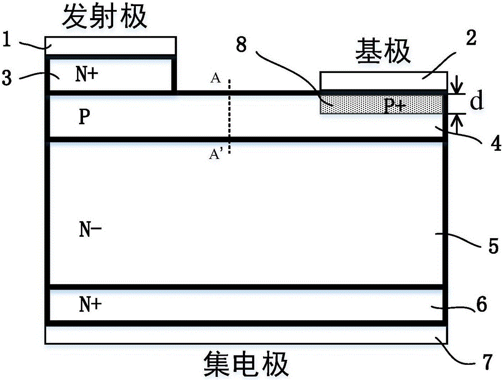
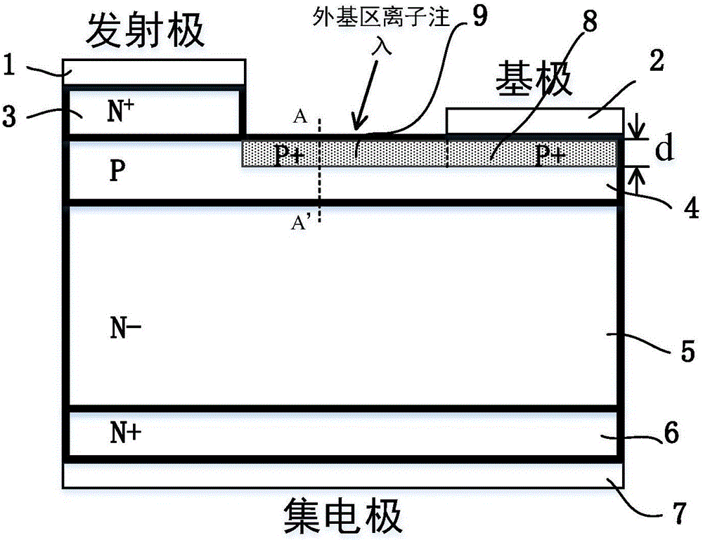
[0018] In order to increase the current gain of SiC BJT in the prior art, it is necessary to reduce the recombination current on the surface of the outer base region between the edge of the emitter 1 mesa and the base ohmic contact 2. There are three main factors affecting the magnitude of the recombination current:

[0019] 1) Defect concentration at the surface of the exogenous base region

[0020] 2) Electron concentration at the surface of the exogenous base region

[0021] 3) Hole concentration at the surface of the extrinsic base region

[0022] Factor 1 depends on the existing material growth and technology level, and factors 2 and 3 may be affected by the design. The present invention is designed to reduce the recombination current on the surface of the outer base region. In the triode ( figure 2 ), the recombination rate of electron-hole pairs mai...


PUM

PropertyMeasurementUnit
Doping concentrationaaaaaaaaaa

Abstract

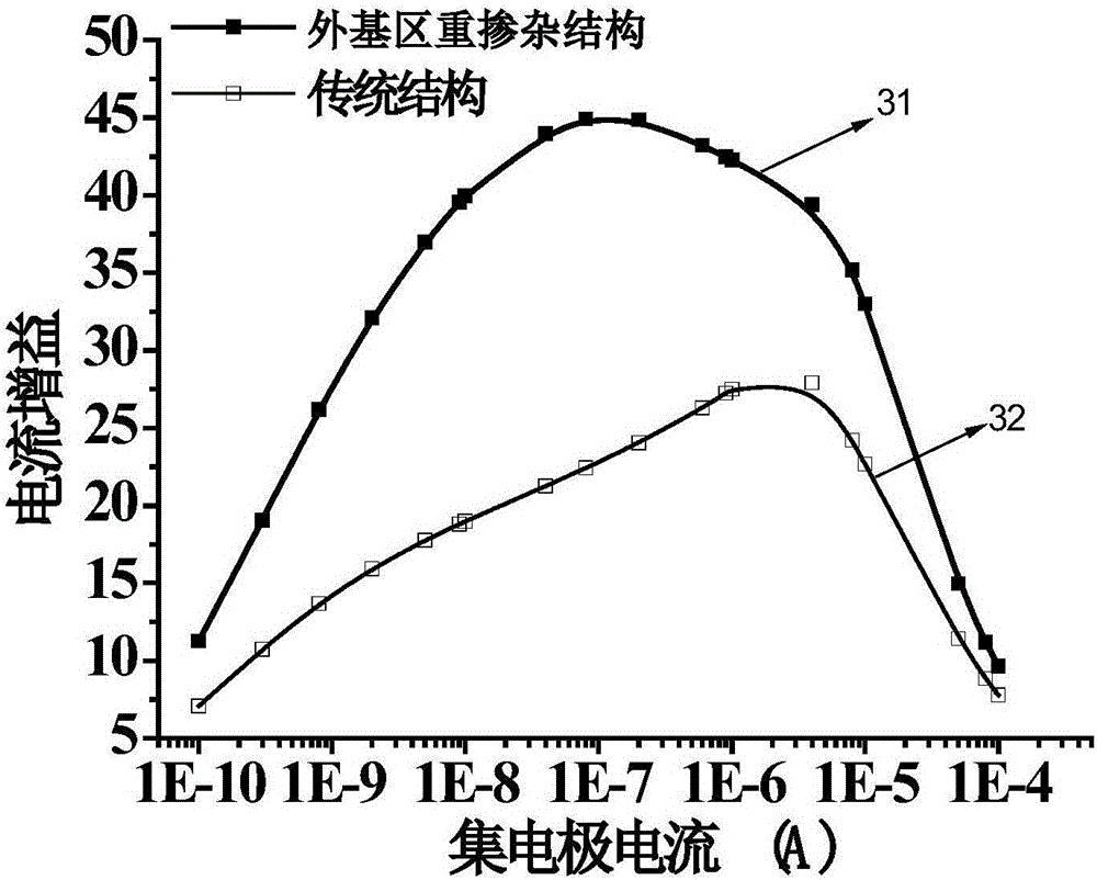
The invention belongs to the technical field of high-power semi-conductors and particularly relates to a silicon carbide BJT (bipolar junction transistor). A second P+ layer 9 is arranged at an outer base region between the edge of an emitter electrode 1 of the BJT and a base electrode ohmic contact of the BJT, is a P-type heavily-doped layer and can be formed with an ion injection process; a P-type base region 4 is a P-type lightly-doped layer, accordingly, an electric field pointing to the heavily-doped layer from the lightly-doped layer is formed between the second P+ layer 9 and the P-type base region 4, the electric filed can prevent minority carriers (electrons) in the base region from diffusing towards the surface of the outer base region, the concentration of the electrons on the surface of the outer base region is reduced, the recombination rate of electrons and holes is reduced, recombination current caused by the interface state is reduced, and the current gain of the device is increased.

Description

technical field [0001] The invention belongs to the technical field of high-power semiconductors, and in particular relates to a silicon carbide bipolar junction transistor. Background technique [0002] The wide bandgap semiconductor material SiC is an ideal material for preparing high-voltage power electronic devices. Silicon carbide (SiC) bipolar junction transistor (BJT) is one of the important normally-off devices. Advantages. Compared with Si-based transistors, SiC BJT has the advantages of lower turn-on voltage and no secondary breakdown phenomenon; SiC BJT avoids the gate drive problem of normally-on device SiC JFET, and does not have the disadvantage of large conduction loss of SiC IGBT , there is no problem that the working conditions of the SiC MOSFET are limited due to the poor stability of the gate dielectric and the low mobility of the channel. [0003] The existence of SiC / SiO2 high interface state will lead to the instability of the gate dielectric of SiC M...

Claims


Application Information

Patent Timeline
IPC IPC(8): H01L29/73H01L29/24H01L29/06
CPCH01L29/73H01L29/0684H01L29/24
Inventor 张有润郭飞施金飞刘影张波
Owner UNIV OF ELECTRONICS SCI & TECH OF CHINA
Learn More