
A method for preparing high-quality znmgbeo thin films

A high-quality, thin-film technology, applied in chemical instruments and methods, from chemically reactive gases, crystal growth, etc., can solve problems such as large lattice, distortion, etc., achieve high luminous performance, ensure quality, and suppress the effect of defect luminescence

Active Publication Date: 2017-11-24
ZHEJIANG UNIV
View PDF3 Cites 0 Cited by
  • Summary
  • Abstract
  • Description
  • Claims
  • Application Information

AI Technical Summary

Problems solved by technology

But Be 2+ The radius (0.31 Å) is small, and a large amount of Be doping will cause large lattice distortion

Method used


Image

  • A method for preparing high-quality znmgbeo thin films

Examples


Embodiment 1

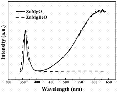
[0015] After cleaning the c-plane sapphire substrate, put it into the molecular beam epitaxy equipment, heat the substrate temperature to 600 °C, and adjust the growth chamber pressure to 2×10 -6 Torr, in radio frequency activated pure O 2 (purity 99.9999%) as O source, activated O 2 The radio frequency power is 350 W; metal Zn (purity 99.9998 %) source, Mg (purity 99.9999 %) source, Be (purity 99.9999 %) source are reaction sources, adjust the heating temperature of Zn source to 280 ℃, Mg source heating temperature to 350 ℃, Be source heating temperature to 880 ℃, grow ZnMgBeO film on c-plane sapphire, growth time is 3 hours, film thickness is about 350 nm.

[0016] Using the same process, ZnMgO thin film was grown on the substrate with metal Zn (purity 99.9998 %) source and Mg (purity 99.9999 %) source as the reaction source.

[0017] figure 1 The room temperature photoluminescence spectra of the ZnMgBeO thin film and the ZnMgO thin film are shown. It can be seen from th...

Embodiment 2

[0020] After cleaning the c-plane sapphire substrate, put it into the molecular beam epitaxy equipment, heat the substrate temperature to 700 °C, and adjust the growth chamber pressure to 3×10 -6 Torr, in radio frequency activated pure O 2 (purity 99.9999%) as O source, activated O 2 The radio frequency power is 350 W; metal Zn (purity 99.9998 %) source, Mg (purity 99.9999 %) source, Be (purity 99.9999 %) source are reaction sources, and the heating temperature of Zn source is adjusted to 280 ℃, and the heating temperature of Mg source is 350 ℃ 1. The Be source was heated to 900 °C, and a ZnMgBeO film was grown on the c-plane sapphire substrate. The growth time was 2 hours, and the film thickness was about 200 nm.

[0021] The prepared ZnMgBeO film has no defect peaks and has good optical properties; the background electron concentration is as low as 2×10 16 cm -3 .

Embodiment 3

[0023] After cleaning the ZnO single crystal substrate, put it into the molecular beam epitaxy equipment, heat the substrate temperature to 500 °C, and adjust the growth chamber pressure to 6×10 -6 Torr, in radio frequency activated pure O 2 (purity 99.9999%) as O source, activated O 2 The radio frequency power is 350 W; metal Zn (purity 99.9998 %) source, Mg (purity 99.9999 %) source, Be (purity 99.9999 %) source are reaction sources, adjust the heating temperature of Zn source to 300 ℃, and the heating temperature of Mg source to 360 ℃ 1. The Be source was heated to 910 °C, and a ZnMgBeO film was grown on a ZnO single crystal substrate. The growth time was 2 hours, and the film thickness was about 300 nm.

[0024] The prepared ZnMgBeO film has no defect peaks and has good optical properties; the background electron concentration is as low as 3×10 16 cm -3 .


PUM


Abstract

A high-quality ZnMgBeO film disclosed by the invention is prepared by virtue of a plasma-assisted molecular beam epitaxy method. The method comprises the following steps of placing a cleaned substrate in a molecular beam epitaxy device, heating the substrate to 400-700 DEG C; by adopting oxygen plasma formed through radio frequency activation of pure O2 as an oxygen source, adjusting the pressure of a growth chamber to 1*10<-6>-1*10<-5>Torr and growing the ZnMgBeO film on the substrate by using pure metals Zn source, Mg source and Be source as reaction sources. By the method disclosed by the invention, the doping concentration of Be is easily controlled, the quality of the film can be effectively guaranteed and the prepared ZnMgBeO film has excellent optical and electrical properties. By doping Be, the defect luminescence can be effectively prevented, the luminescence property of the ZnMgBeO film is greatly increased and meanwhile, the background electron concentration of the ZnMgBeO film is decreased; therefore, a foundation is laid for preparation of a ZnO-based optoelectronic device having high luminescent property.

Description

technical field [0001] The invention relates to a growth method of a ZnO-based thin film, especially a preparation method of a high-quality ZnMgBeO thin film. Background technique [0002] ZnO, as a semiconductor material with direct bandgap and wide bandgap, has a bandgap of 3.37 eV at room temperature and an exciton binding energy as high as 60 meV. These characteristics make ZnO-based materials have great application potential in the field of ultraviolet optoelectronics. In order to realize its wide application, two key problems need to be solved: the preparation of n-type and p-type ZnO with excellent performance; the growth of quantum well structure to improve the efficiency of optoelectronic devices. At present, ZnMgO is considered to be a suitable barrier material for ZnO-based quantum wells, mainly because Mg 2+ Radius (0.57 Å) vs. Zn 2+ The radius (0.60 Å) is close to that in ZnMgO alloys, with the increase of Mg content, the forbidden band width increases without...

Claims


Application Information

Patent Timeline
Patent Type & Authority Patents(China)
IPC IPC(8): C30B25/16
Inventor 叶志镇陈珊珊潘新花黄靖云吕斌
Owner ZHEJIANG UNIV
Learn More