
MOSFET with high-resistance layer, preparation method of MOSFET, and power transistor module

A high-resistance layer and epitaxial layer technology, applied in the direction of semiconductor devices, semiconductor/solid-state device manufacturing, electrical components, etc., can solve the problems of increasing on-resistance, decreasing power quality factor, and decreasing device power quality factor. The effect of electron concentration, increasing breakdown voltage, and reducing leakage current

Active Publication Date: 2021-08-24
UNIV OF SCI & TECH OF CHINA
View PDF4 Cites 0 Cited by
  • Summary
  • Abstract
  • Description
  • Claims
  • Application Information

AI Technical Summary

Problems solved by technology

[0004] In the design of MOSFET, increasing the distance between the drain and the gate of the MOSFET and reducing the channel doping concentration can reduce the leakage current and increase the breakdown voltage, but it will lead to a significant increase in the on-resistance and increase in the conduction loss. Even lead to a decrease in the power quality factor of the device
If only from the perspective of reducing the on-resistance, reducing the gate-drain spacing and increasing the channel doping concentration may also lead to a decrease in power quality factor
In addition, in order to prevent accidental current paths in the circuit when the circuit fails in practical applications, normally-off MOSFETs are more likely to be used in practical applications
However, due to lack of p-type doping method in gallium oxide, normally-off gallium oxide MOSFET is not easy to realize

Method used


Image

  • MOSFET with high-resistance layer, preparation method of MOSFET, and power transistor module
  • MOSFET with high-resistance layer, preparation method of MOSFET, and power transistor module
  • MOSFET with high-resistance layer, preparation method of MOSFET, and power transistor module

Examples


Embodiment Construction

[0023] In order to make the object, technical solution and advantages of the present invention clearer, the present invention will be further described in detail below in conjunction with specific embodiments and with reference to the accompanying drawings.

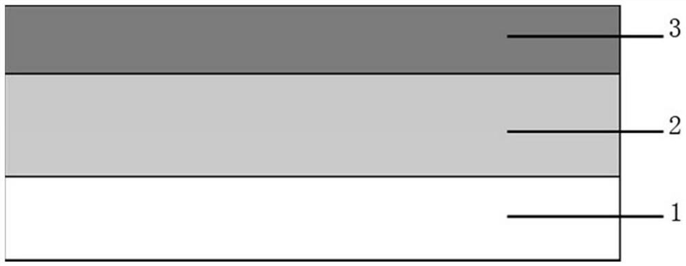
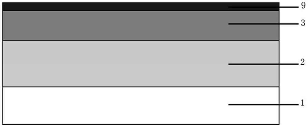
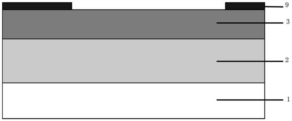
[0024] The invention provides a MOSFET with a high resistance layer, Figure 8 A schematic diagram of the structure of a MOSFET with a high-resistance layer is schematically shown. Including semi-insulating substrate layer 1, buffer layer 2, epitaxial layer 3, high resistance layer 4; source electrode 5, drain electrode 6, gate electrode 7; wherein, semi-insulating substrate layer 1, buffer layer 2, epitaxial layer 3 from bottom to top Arranged in sequence; the source electrode 5 and the drain electrode 6 are arranged on the upper surface of the epitaxial layer 3, and the source electrode 5 and the drain electrode 6 form ohmic contact with the epitaxial layer 3; a gate dielectric 8 is arranged on the upper surface of the ...


PUM


Abstract

The invention discloses an MOSFET with a high-resistance layer, a preparation method of the MOSFET and a power transistor module, and the MOSFET with the high-resistance layer comprises a semi-insulating substrate layer, a buffer layer, an epitaxial layer and the high-resistance layer, a source electrode, a drain electrode, and a gate electrode, wherein the semi-insulating substrate layer, the buffer layer and the epitaxial layer are sequentially arranged from bottom to top; the source electrode and the drain electrode are arranged on the upper surface of the epitaxial layer, and the source electrode, the drain electrode and the epitaxial layer form ohmic contact; a gate medium is arranged on the upper surface of the non-ohmic contact area of the epitaxial layer; the gate electrode is arranged on the upper surface of the gate dielectric; a high-resistance layer is arranged in a non-ohmic contact area between the gate electrode and the drain electrode in the epitaxial layer; the high-resistance layer comprises N-type gallium oxide, and the carrier concentration of the high-resistance layer is 0-1 * 10 < 16 > cm <-3 >.

Description

technical field [0001] The invention relates to the technical field of semiconductors, in particular to a MOSFET with a high-resistance layer, a preparation method thereof, and a power transistor module. Background technique [0002] MOSFET (Metal Oxide Semiconductor Field Effect Transistor) is a switching device that can control the magnitude of the current between the drain and source by changing the voltage applied to the gate. Key performance metrics for MOSFETs include on-resistance, on-state output current, off-state leakage current, and breakdown voltage. However, the conduction characteristics and the off-state characteristics of the device are mutually restricted, and the improvement of the off-state characteristics often comes at the cost of a decrease in the conduction characteristics. Therefore, it is difficult to prepare a device with high power quality factor that simultaneously has low on-resistance, large output current, high breakdown voltage, and low leaka...

Claims


Application Information

Patent Timeline
Patent Type & Authority Applications(China)
IPC IPC(8): H01L29/78H01L29/06H01L21/34H05B45/37
CPCH01L29/78H01L29/0607H01L29/0611H01L21/34H01L29/66969H05B45/37
Inventor 徐光伟刘琦周选择龙世兵赵晓龙
Owner UNIV OF SCI & TECH OF CHINA
Learn More