FinFET device and manufacturing method thereof

A device manufacturing method and device technology, applied in semiconductor/solid-state device manufacturing, semiconductor devices, electrical components, etc., can solve the problems of channel surface damage, increase process complexity, and difficulty in controlling impurity distribution, so as to suppress punch-through current, The effect of increasing process complexity and improving device performance

Inactive Publication Date: 2016-06-01
INST OF MICROELECTRONICS CHINESE ACAD OF SCI
View PDF4 Cites 4 Cited by
  • Summary
  • Abstract
  • Description
  • Claims
  • Application Information

AI Technical Summary

Problems solved by technology

The current general doping method is ion implantation to form the required heavily doped region. However, the depth of ion implantation is difficult to control precisely, and at the same time it will cause damage to the channel surface. In order to eliminate the damage, a thin layer is usually formed on the channel surface. Oxide layer, increasing process complexity
At the same time, the distribution of impurities is difficult to control, and it is difficult to accurately form an ultra-steep inverted well at the bottom of the channel. Instead, impurities and defects will be introduced into the channel, which will affect the subthreshold characteristics of the device.

Method used


Image

  • FinFET device and manufacturing method thereof
  • FinFET device and manufacturing method thereof
  • FinFET device and manufacturing method thereof

Examples


Embodiment Construction

[0026] In order to make the object, technical solution and advantages of the present invention clearer, the embodiments of the present invention will be described in detail below with reference to the accompanying drawings.

[0027] Embodiments of the present invention are described in detail below, examples of which are shown in the drawings, wherein the same or similar reference numerals designate the same or similar elements or elements having the same or similar functions throughout. The embodiments described below by referring to the figures are exemplary only for explaining the present invention and should not be construed as limiting the present invention.

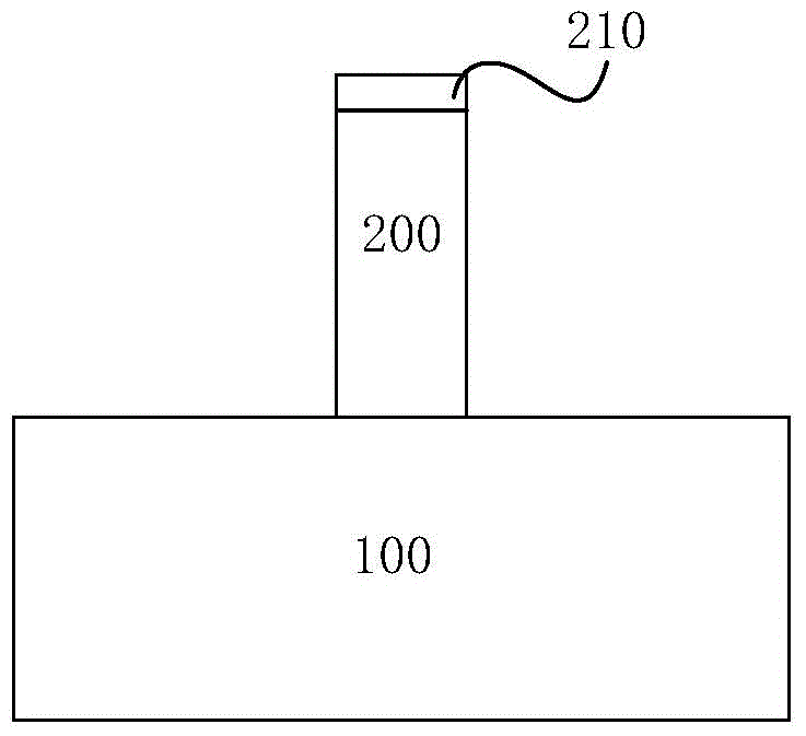
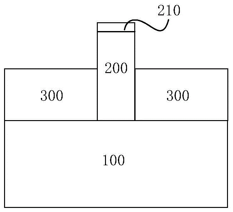
[0028] The present invention provides a FinFET device, comprising: a substrate 100; a fin 200 located above the substrate 100; shallow trench isolation 300 located on the substrate 100 on both sides of the fin 200; an isolation oxide layer 400, located in the fin 200, the top of which is flush with the shallow trenc...


PUM


Abstract

The invention provides an FinFET device and a manufacturing method thereof. The manufacturing method comprises the steps of a. providing a substrate on which a fin is disposed; b. forming shallow trench isolation on the substrate and at two sides of the fin; c. forming a protective mask at the two sides of the fin; d. thinning the shallow trench isolation to expose the fin partially; e. forming an isolation oxide layer on the fin that is not covered by the shallow trench isolation and the protective mask; f. removing the protective mask, and thickening the shallow trench isolation so as to be level with the isolation oxide layer; and g. forming a source and drain region, a gate structure and an interlayer dielectric layer in sequence on the thickened shallow trench isolation. According to the invention, the method of forming the oxide isolation layer in a region below a device trench allows a bulk silicon device have similar performance to an SOI device, and the punch-through current can be effectively suppressed without affecting other parameters of the device.

Description

technical field [0001] The present invention relates to a method for manufacturing a semiconductor device, in particular to a method for manufacturing a FinFET. technical background [0002] As the size of the semiconductor device is scaled down, there arises a problem that the threshold voltage decreases with the decrease of the channel length, that is, a short channel effect is generated in the semiconductor device. To meet the challenges from semiconductor design and manufacturing, led to the development of Fin Field Effect Transistor, or FinFET. [0003] Channel punch-through effect (Channelpunch-througheffect) is a phenomenon that the source junction and the depletion region of the drain junction of the field effect transistor are connected. When the channel is penetrated, the potential barrier between the source and the drain is significantly reduced, and a large number of carriers are injected from the source to the channel, and drift through the space charge region ...

Claims


Application Information

Patent Timeline
Patent Type & Authority Applications(China)
IPC IPC(8): H01L21/336H01L29/78H01L29/06
CPCH01L29/66795
Inventor 刘云飞尹海洲李睿
Owner INST OF MICROELECTRONICS CHINESE ACAD OF SCI
Why Eureka
Try Eureka