Indium oxide sintered body and indium oxide transparent conductive film

一种透明导电膜、烧结体的技术,应用在氧化物导体、绝缘载体上的导电层、非金属导体等方向,能够解决长波长区域透射率低等问题,达到低电阻率、有效利用、提高转换效率的效果

Active Publication Date: 2012-09-12
JX NIPPON MINING & METALS CORP
View PDF5 Cites 3 Cited by
  • Summary
  • Abstract
  • Description
  • Claims
  • Application Information

AI Technical Summary

Problems solved by technology

However, all the results are values ​​obtained under very high temperature conditions such as a substrate temperature of 400°C. Therefore, when the resistivity is low, the carrier concentration is also high, so the transmittance in the long wavelength region is expected to be low, but This document only shows measurement results up to a wavelength of 900nm

Method used


Image

  • Indium oxide sintered body and indium oxide transparent conductive film

Examples


Embodiment 1

[0070] Indium oxide (In 2 o 3 ) raw material powder and niobium oxide (Nb 2 o 5 ) powder, mixed in air at 3000 rpm for 3 minutes rotation time using a high-speed mixer.

[0071] Then, the mixed powder was put into an attritor together with zirconia microspheres, and finely pulverized at a rotation speed of 300 rpm for 3 hours to adjust the average particle diameter (D50) to 0.8 μm. The amount of water was adjusted to form finely pulverized raw materials into a slurry with a solid content of 50%, and the inlet temperature was set to 200°C, and the outlet temperature was set to 120°C for granulation.

[0072] Then, at 600kgf / cm 2 After the granulated powder is pressed and shaped under the condition of keeping the surface pressure for 1 minute, use an isostatic pressing device (CIP) at 1800kgf / cm 2 The surface pressure is maintained for 1 minute for forming. Then, this molded product was held in an electric furnace at 1550° C. for 20 hours in an oxygen atmosphere to perform...

Embodiment 2~4、 comparative example 1~2

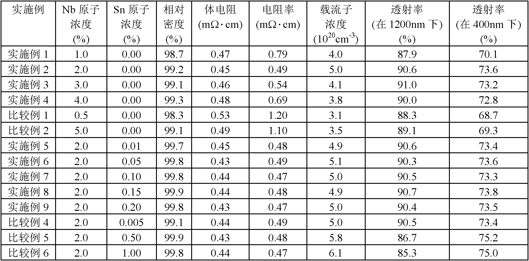
[0078] The method of manufacturing the sintered body and the method of manufacturing the transparent conductive film were the same as in Example 1, except that the ratio of the atomic concentration (number of atoms) of niobium was changed. That is, in Example 2, the atomic concentration of niobium was 2.0%, in Example 3 the atomic concentration of niobium was 3.0%, and in Example 4 the atomic concentration of niobium was 4.0%. In addition, in Comparative Example 1, the atomic concentration of niobium was 0.5%, and in Comparative Example 2, the atomic concentration of niobium was 5.0%.

[0079] Table 1 shows the results of properties of the obtained sintered body and film. From these results, it can be seen that when the ratio of the atomic number of niobium is out of the range of 1 to 4%, the specific resistance becomes high, so that the property as a transparent conductive film is not preferable. In addition, it can be seen that although tin is not added, the relative densit...

Embodiment 5~9、 comparative example 4~6

[0083] The production method of the sintered body and the production method of the transparent conductive film were the same as in Example 1, except that the ratio of the atomic number of niobium was set to 2.0%, and the ratio of the atomic concentration of tin was changed. That is, the atomic concentration of tin in Example 5 is 0.01%, the atomic concentration of tin in Example 6 is 0.05%, the atomic concentration of tin in Example 7 is 0.10%, and the atomic concentration of tin in Example 8 is The atomic concentration of tin in Example 9 was 0.15%. In addition, the atomic concentration of tin in Comparative Example 4 was 0.005%, the atomic concentration of tin in Comparative Example 5 was 0.50%, and the atomic concentration of tin in Comparative Example 6 was 1.00%. The results of the characteristics of the obtained sintered bodies and films are also listed in Table 1.

[0084] From these results, it can be seen that although the relative density is 98.7% when the tin conce...


PUM

PropertyMeasurementUnit
relative densityaaaaaaaaaa
electrical resistivityaaaaaaaaaa

Abstract

Disclosed is an indium oxide sintered body which contains niobium as an additive. The indium oxide sintered body is characterized in that: the ratio of the number of niobium atoms relative to the total number of atoms of all the metal elements contained in the sintered body is within the range of 1-4%; the relative density thereof is not less than 98%; and the bulk resistivity thereof is not more than 0.9 m[omega]cm. The indium oxide sintered body has high transmittances in short wavelength and long wavelength ranges, since the carrier concentration thereof is not too high although the resistivity thereof is low. Also disclosed is an indium oxide transparent conductive film.

Description

technical field [0001] The present invention relates to an indium oxide-based oxide sintered body and an indium oxide-based transparent conductive film. Background technique [0002] As a transparent conductive film, tin-doped indium oxide (hereinafter referred to as ITO) is widely used as an electrode material for FPD (Flat Panel Display) and the like due to its excellent characteristics of low resistivity and high transmittance. [0003] Transparent conductors are used in various applications other than flat panel displays. Among them, in recent years, demand has been increasing as a material for window layer electrodes (layer electrodes) on the light incident surface side of solar cells. [0004] The spectral sensitivity of solar cells is up to about 1200nm for crystalline silicon type and up to about 1300nm for CIGS (Cu-In-Ga-Se system) type, so high transmittance is required in such a long wavelength region. In addition, in an amorphous silicon solar cell, the spectral...

Claims


Application Information

Patent Timeline
Patent Type & Authority Applications(China)
IPC IPC(8): C04B35/00H01B5/14C23C14/34H01B1/08
CPCC03C17/245C04B35/01C04B35/6261C04B35/62635C04B35/62695C04B2235/3251C04B2235/3286C04B2235/3293C04B2235/5409C04B2235/5436C04B2235/5445C04B2235/604C04B2235/6567C04B2235/77C04B2235/9653C23C14/086C23C14/3414C23C30/00H01B1/08C04B35/495C23C14/34H01B5/14
Inventor 生泽正克高见英生
Owner JX NIPPON MINING & METALS CORP
Why Eureka
Try Eureka