

A three-stage transconductance amplifier
A technology of transconductance amplifier and input structure, used in amplifiers, differential amplifiers, amplifiers with semiconductor devices/discharge tubes, etc., can solve the problems of reducing the frequency of the main pole, increasing the layout area, and low voltage slew rate of the transconductance amplifier. , to maximize, increase unity gain bandwidth, and increase voltage slew rate
- Summary
- Abstract
- Description
- Claims
- Application Information
AI Technical Summary
Problems solved by technology
Method used
Image

Examples
Embodiment Construction
[0026] The preferred embodiments of the present invention will be described in detail below in conjunction with the accompanying drawings; it should be understood that the preferred embodiments are only for illustrating the present invention, rather than limiting the protection scope of the present invention.
[0027] In order to describe the above problems in more detail, first analyze the working principle of the two three-stage transconductance amplifiers and the advantages and disadvantages of frequency compensation technology.
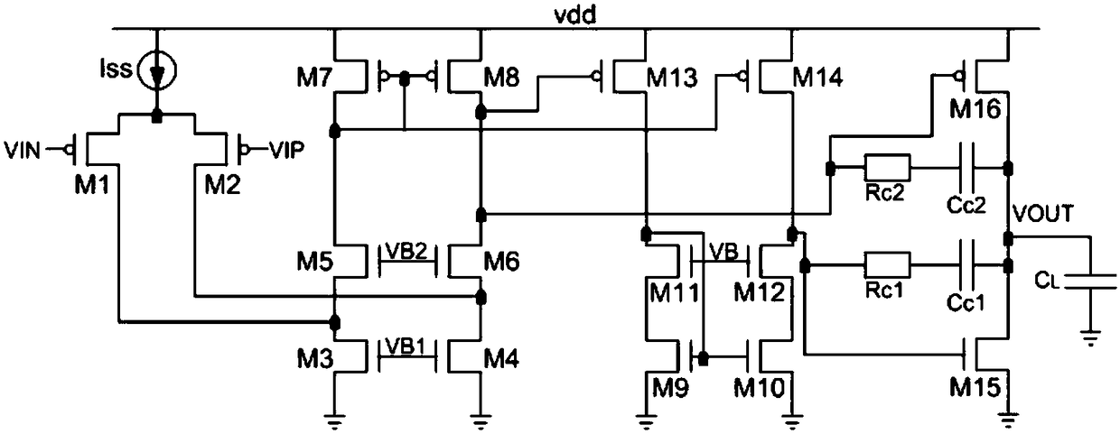
[0028] Such as figure 1 A schematic diagram of a traditional three-stage transconductance amplifier RC compensation technology (referred to as the structure [1]) is given. The two compensation networks are respectively composed of compensation resistor Rc1 / compensation capacitor Cc1 and compensation resistor Rc2 / compensation capacitor Cc2 in series. One end of the compensation resistor Rc1 is connected to the compensation capacitor Cc1, the other ...
PUM
 Abstract
Description
Claims
Application Information