Preparation of sidewall reflector DUV LED based on3D printing

A 3D printing and mirror technology, applied in electrical components, circuits, semiconductor devices, etc., can solve problems such as limited effect, and achieve the effect of improving production efficiency, improving light output efficiency, and simple production process

Active Publication Date: 2016-08-31
TAIYUAN UNIV OF TECH
View PDF4 Cites 8 Cited by
  • Summary
  • Abstract
  • Description
  • Claims
  • Application Information

AI Technical Summary

Problems solved by technology

However, traditional patterned substrates, surface roughening, anti-reflection layers, high-reflective mirrors and other technologies have limited effect on improving the light extraction efficiency of deep ultraviolet LEDs.

Method used


Image

  • Preparation of sidewall reflector DUV LED based on3D printing
  • Preparation of sidewall reflector DUV LED based on3D printing
  • Preparation of sidewall reflector DUV LED based on3D printing

Examples


Embodiment 1

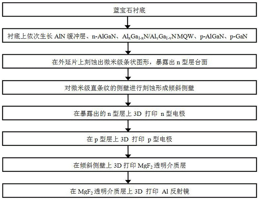
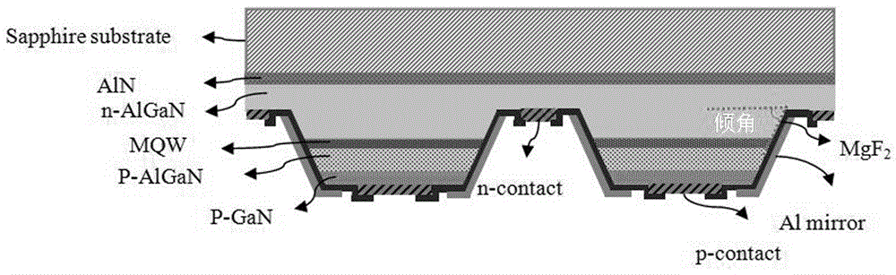
[0027] Sapphire is provided as a substrate.

[0028] Step 1: sequentially grow AlN buffer layer, n-AlGaN layer, multi-period Al x Ga 1-x N / Al y Ga 1-y Epitaxial wafer of N active layer (where x

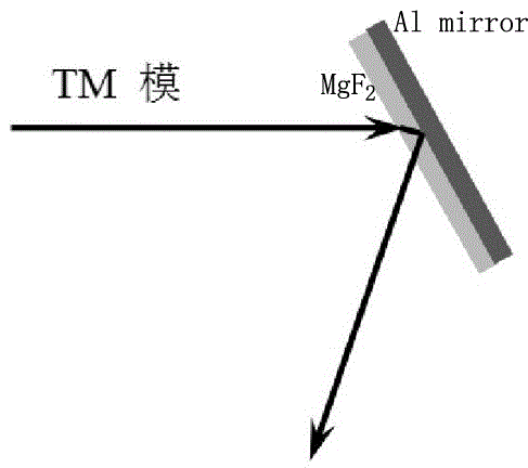
[0029] Step 2: Uniformly and parallelly etch micron-scale straight stripes on the epitaxial wafer, the etching depth reaches the n-AlGaN layer, and the distribution density of straight stripes is 5 pieces / mm 2 , and etch the sidewalls formed by the straight stripes to form inclined sidewalls with an inclination angle of 80°.

[0030] Step 3: Write the motion path program of each 3D printing head, put the cleaned epitaxial wafer as a substrate into the 3D printer; use a single or array 3D N-type electrode printing head to print n-type on the exposed n-AlGaN layer electrode.

[0031] Use a single or array 3D P-type electrode print head to print p-type electrodes on the p-GaN contact layer between the straight stripes, the p-type electrode...

Embodiment 2

[0035] Sapphire is provided as a substrate.

[0036] Step 1: sequentially grow AlN buffer layer, n-AlGaN layer, multi-period Al x Ga 1-x N / Al y Ga 1-y Epitaxial wafer of N active layer (where x

[0037] Step 2: Uniformly and parallelly etch micron-scale straight stripes on the epitaxial wafer, the etching depth reaches the n-AlGaN layer, and the distribution density of straight stripes is 50 pieces / mm 2 , and etch the sidewalls formed by the straight stripes to form inclined sidewalls with an inclination angle of 20°.

[0038] Step 3: Write the motion path program of each 3D printing head, put the cleaned epitaxial wafer as a substrate into the 3D printer; use a single or array 3D N-type electrode printing head to print n-type on the exposed n-AlGaN layer electrode.

[0039] Use a single or array 3D P-type electrode print head to print p-type electrodes on the p-GaN contact layer between the straight stripes, the p-type electrod...

Embodiment 3

[0043] Sapphire is provided as a substrate.

[0044] Step 1: sequentially grow AlN buffer layer, n-AlGaN layer, multi-period Al x Ga 1-x N / Al y Ga 1-y Epitaxial wafer of N active layer (where x

[0045] Step 2: Uniformly and parallelly etch micron-scale straight stripes on the epitaxial wafer, the etching depth reaches the n-AlGaN layer, and the distribution density of straight stripes is 30 pieces / mm 2 , and etch the sidewalls formed by the straight stripes to form inclined sidewalls with an inclination angle of 50°.

[0046] Step 3: Write the motion path program of each 3D printing head, put the cleaned epitaxial wafer as a substrate into the 3D printer; use a single or array 3D N-type electrode printing head to print n-type on the exposed n-AlGaN layer electrode.

[0047] Use a single or array 3D P-type electrode print head to print p-type electrodes on the p-GaN contact layer between the straight stripes, the p-type electrod...


PUM


Abstract

The invention belongs to the field of photoelectronic devices, in particular to preparation of a sidewall reflector DUV LED based on3D printing. The preparation comprises the steps of: providing an epitaxial wafer which is generated by MOCVD or MBE and comprises an AlN buffer layer, an n-AlGaN layer, a multi-period Al<x>Ga<1-x>N / Al<y>Ga<1-y>N active layer (where x<y), a p-AlGaN layer and a p-GaN contact layer; etching the epitaxial layer to form micron-grade straight stripes with inclined side walls; taking the epitaxial layer as a substrate; and printing electrodes, a UV light transmission medium layer and a reflector reflective layer in a 3D manner. The UV light transmission medium layer serves as an electric insulating layer between the active layer and a metal reflector and serves as an electric passivation layer of the side walls, and the UV light transmission medium layer and the reflector reflective layer are combined together to form an omni-directional reflector which can reflect TM mode lateral reflected light to the substrate, thereby increasing light emitting efficiency. In addition, the 3D printing production process is simple, and production efficiency can be effectively increased.

Description

technical field [0001] The invention belongs to the field of optoelectronic devices, in particular to a DUV LED based on 3D printing to prepare a side wall reflector. Background technique [0002] Ultraviolet light-emitting diodes (LEDs) have the advantages of environmental protection and non-toxicity, low power consumption, small size and long life, and meet the requirements of environmental protection and energy saving in the new era. The emission wavelength of AlGaN-based LEDs can cover the range of 210nm-360nm, of which 210nm-300nm belongs to the deep ultraviolet band. Deep ultraviolet LEDs have great application value in printing, medical treatment, purification, detection, data storage and lighting. [0003] Compared with GaN-based blue LEDs, deep-UV LEDs with wavelengths shorter than 300nm generally have lower luminous efficiencies. As the light-emitting wavelength of AlGaN-based LEDs gradually shortens, the Al composition in the light-emitting layer AlGaN will incr...

Claims


Application Information

Patent Timeline
Patent Type & Authority Applications(China)
IPC IPC(8): H01L33/60
CPCH01L33/60
Inventor 卢太平朱亚丹周小润许并社
Owner TAIYUAN UNIV OF TECH
Why Eureka
Try Eureka