Surface-Emitting Semiconductor Laser, Surface-Emitting Semiconductor Laser Array, Surface-Emitting Semiconductor Laser Device, Optical Transmission Device, And Information Processing Device

A semiconductor, surface emitting technology, applied in semiconductor lasers, lasers, laser parts, etc., can solve the problems of reducing carriers, high device resistance, increasing carrier penetration, etc., and achieves the effect of reducing oxidation and easy resonance.

Active Publication Date: 2016-08-31
FUJIFILM BUSINESS INNOVATION CORP
View PDF9 Cites 0 Cited by
  • Summary
  • Abstract
  • Description
  • Claims
  • Application Information

AI Technical Summary

Problems solved by technology

However, in this case, if the thickness of the carrier blocking layer is large, the resistance of the device can become too high
On the other hand, reducing the thickness of the carrier

Method used


Image

  • Surface-Emitting Semiconductor Laser, Surface-Emitting Semiconductor Laser Array, Surface-Emitting Semiconductor Laser Device, Optical Transmission Device, And Information Processing Device
  • Surface-Emitting Semiconductor Laser, Surface-Emitting Semiconductor Laser Array, Surface-Emitting Semiconductor Laser Device, Optical Transmission Device, And Information Processing Device
  • Surface-Emitting Semiconductor Laser, Surface-Emitting Semiconductor Laser Array, Surface-Emitting Semiconductor Laser Device, Optical Transmission Device, And Information Processing Device

Examples


Embodiment Construction

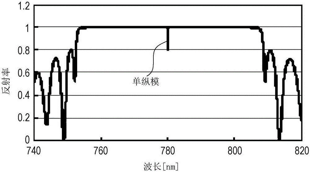
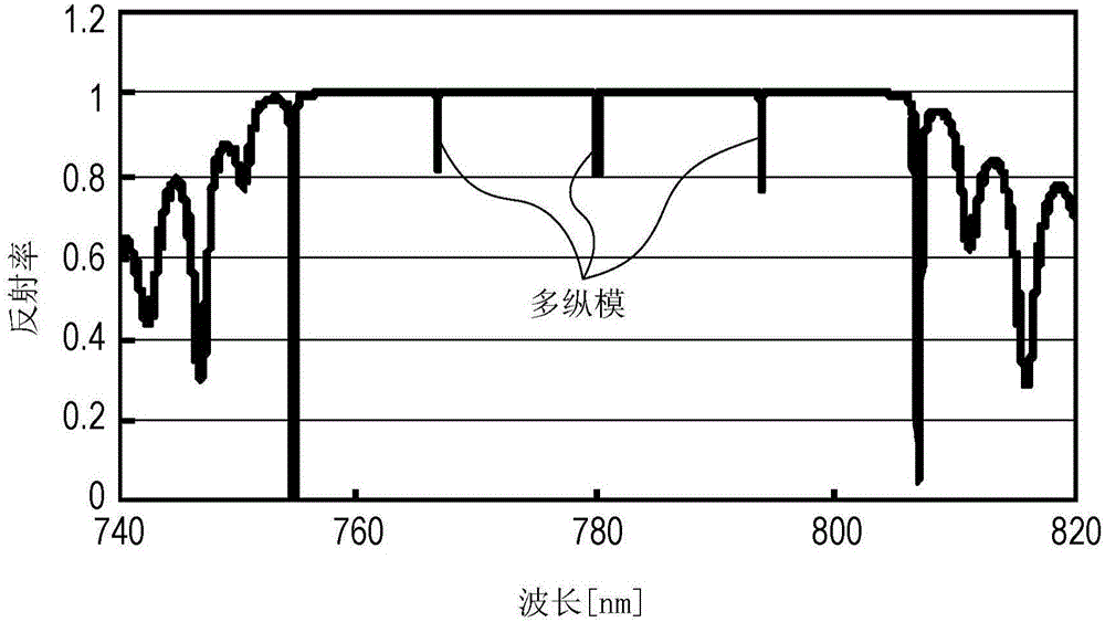
[0045] Exemplary embodiments of the present invention are described below with reference to the accompanying drawings. Surface emitting semiconductor lasers (ie, vertical cavity surface emitting lasers, hereinafter abbreviated as "VCSEL") have been used as light sources for communication devices or image forming devices. In order to further increase the printing speed in the future, there is a demand for single-mode, high light output VCSEL. In order to realize single-mode (ie, fundamental transverse mode) operation using the oxidation-constrained type structure of the related art, it is necessary to set the diameter of the oxidation orifice to be 2 to 3 μm. However, setting the diameter of the oxidation aperture to 2 to 3 μm makes it difficult to uniformly achieve a single-mode light output of 3 mW or more. Setting the diameter of the oxidation aperture larger than 2 to 3 μm enables high light output, but disadvantageously, multi-mode (ie, higher transverse mode) oscillation...


PUM


Abstract

A surface-emitting semiconductor laser includes a substrate; a first semiconductor multilayer film reflector stacked on the substrate; an active region stacked on or above the first semiconductor multilayer film reflector; a second semiconductor multilayer film reflector stacked on or above the active layer; a cavity extension region interposed between the first semiconductor multilayer film reflector and the active region or between the second semiconductor multilayer film reflector and the active region; and a carrier block layer interposed between the cavity extension region and the active region. The carrier block layer includes a first carrier block layer and a second carrier block layer. The first and second carrier block layers have a larger band gap than the active region and the cavity extension region. The first carrier block layer has a larger band gap than the second carrier block layer.

Description

technical field [0001] The invention relates to a surface-emitting semiconductor laser, a surface-emitting semiconductor laser array, a surface-emitting semiconductor laser device, an optical transmission device and an information processing device. Background technique [0002] A surface-emitting semiconductor laser is a light-emitting device capable of emitting a laser beam in a direction perpendicular to a substrate, and thus is easily formed in a two-dimensional array. Thus, surface emitting semiconductor lasers have been increasingly used as light sources for printers, image forming apparatuses, optical communications, and the like. [0003] A method has been studied in which there is a loss difference between the fundamental transverse mode and higher transverse modes in order to operate a surface emitting type semiconductor laser in a single transverse mode and a single longitudinal mode. One study disclosed a surface-emitting semiconductor laser with a large chamber...

Claims


Application Information

Patent Timeline
IPC IPC(8): H01S5/183H01S5/343H01S5/42
CPCH01S5/02212H01S5/18313H01S5/18358H01S5/2009H01S5/343G02B19/0052H01S5/02251G02B26/10
Inventor 近藤崇村上朱实武田一隆城岸直辉早川纯一朗樱井淳
Owner FUJIFILM BUSINESS INNOVATION CORP
Why Eureka
Try Eureka