Nand Flash memory array based storage control apparatus

A memory array and storage control technology, applied in static memory, read-only memory, information storage, etc., can solve the problems of low speed, poor integration, and reduced data reliability, so as to suppress the inherent bit error rate, solve large-capacity, The effect of error-free data access and access control

Active Publication Date: 2016-09-07
XIDIAN UNIV
View PDF6 Cites 17 Cited by
  • Summary
  • Abstract
  • Description
  • Claims
  • Application Information

AI Technical Summary

Problems solved by technology

[0003] Currently commercially available solid state disks (Solid State Disk, SSD) are products of this digital acquisition and playback device. However, solid state disk products have small capacity, low speed, and poor integration, which cannot meet the storage and playback requirements of high-speed real-time signal processing systems. There are many technical difficulties in the development of special storage devices based on semiconductor solid-state storage: (1) input and output synchronization problems caused by operating multiple semiconductor memories at the same time; Blocks will affect data storage, manage bad blocks without affecting read and write performance, and prolong the service life of storage devices; (3) The inherent bit error defects of Nand structure memory greatly reduce data reliability. Use error control coding to reduce or even eliminate the impact of bit errors; (4) In order to prolong the trouble-free time of storage devices, it is crucial and difficult to control the load balancing of all storage semiconductors on the device; (5) In dedicated In the device, the speed requirements for storage and reading are particularly important, so a number of technologies are required to ensure high-speed operation

Method used


Image

  • Nand Flash memory array based storage control apparatus
  • Nand Flash memory array based storage control apparatus
  • Nand Flash memory array based storage control apparatus

Examples


Embodiment Construction

[0022] In the description of the present invention, unless otherwise specified and limited, the term "connection" should be understood in a broad sense, for example, it can be a fixed connection, a detachable connection, or an integral connection; it can be a mechanical connection, or It is an electrical connection; it can be a direct connection, or a connection through an intermediary, or an internal communication between two components. Those of ordinary skill in the art can understand the specific meanings of the above words in the present invention according to specific situations.

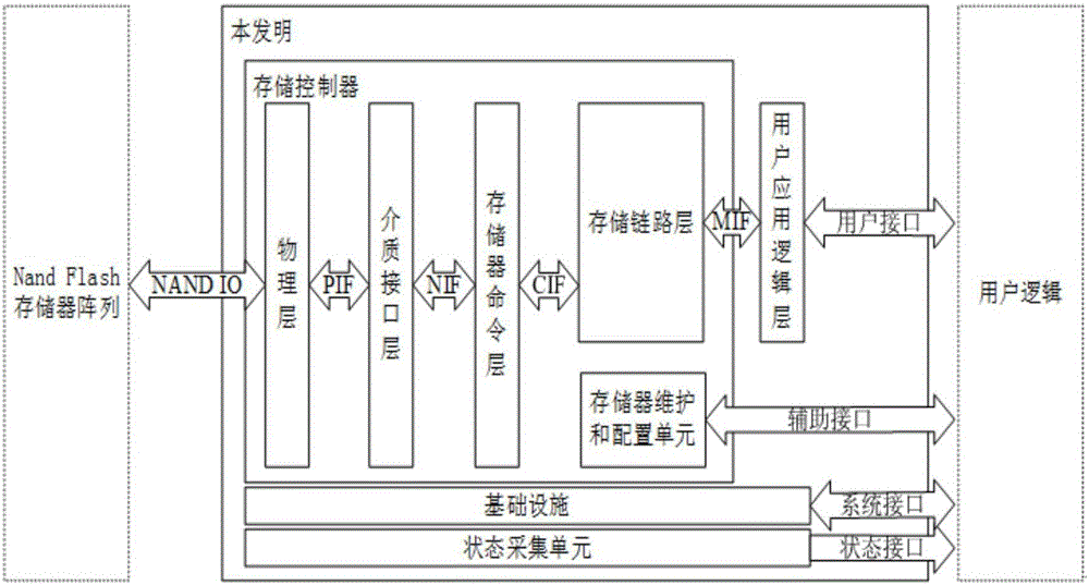
[0023] refer to figure 1, is a kind of storage control device schematic diagram based on Nand Flash memory array of the present invention; Described storage control device based on Nand Flash memory array adopts Verilog language as description means, and then carry out logical description to the storage control device based on Nand Flash memory array , and adopt the FPGA (XC6VLX240T-1ff1759) ...


PUM


Abstract

The present invention discloses a Nand Flash memory array based storage control apparatus. The Nand Flash memory array based storage control apparatus comprises: a Nand Flash memory array, a storage controller, a user application logic layer, user logic, an infrastructure, and a state acquisition unit. The Nand Flash memory array obtains an operation instruction; a physical layer obtains an operation time sequence; a media interface layer obtains a parsed reconstruction data stream; a memory command layer obtains a decomposed Nand Flash operation data stream and a command interface time sequence; a storage link layer obtains data fames in accordance with the command interface time sequence and a decoded command interface time sequence; the user layer obtains a register configuration command, clock and reset signals, a work state, the operation instruction data stream; a memory maintenance and configuration unit obtains parsed register configuration command; the infrastructure obtains the clock and reset signals; the state acquisition unit obtains the work state; the user application logic layer obtains a data format and an operation format required by a memory control interface; and the state acquisition unit obtains a user logic operation command.

Description

technical field [0001] The invention belongs to the technical field of high-speed data recording, and in particular relates to a storage control device based on a Nand Flash solid-state memory array, which is used for functional verification and performance testing using a field programmable gate array (Field Programable Gate Array, FPGA) as a verification test platform , provided for use in the form of IP cores. Background technique [0002] High-speed data recording technology is one of the key technologies in many fields at home and abroad. This high-speed data recording technology includes detection, investigation, monitoring, equipment testing and field debugging. The original high-speed digital signal data flow in the engineering environment needs to be completely recorded in order to Fault diagnosis, scene review and data archiving work will be carried out later, and the actual application environment often has large temperature differences, dusty or strong vibrations...

Claims


Application Information

Patent Timeline
Patent Type & Authority Applications(China)
IPC IPC(8): G11C16/10
Inventor 苏涛徐杰张辉马文锐
Owner XIDIAN UNIV
Why Eureka
Try Eureka