Plane gate IGBT and manufacturing method therefor

A planar gate and gate electrode technology, applied in the field of planar gate insulated gate bipolar transistors and insulated gate bipolar transistors, can solve the problems of increasing device switching loss, reducing device switching speed, device oscillation, etc.

Inactive Publication Date: 2016-09-07
UNIV OF ELECTRONIC SCI & TECH OF CHINA
View PDF4 Cites 11 Cited by
  • Summary
  • Abstract
  • Description
  • Claims
  • Application Information

AI Technical Summary

Problems solved by technology

The gate structure on the upper part of the wide JFET region still brings large device capacitance, especially the gate-collector capacitance, which reduces the switching speed of the device, increases the switching loss of the device, and improves the ability of the device gate drive circuit requirement

Method used


Image

  • Plane gate IGBT and manufacturing method therefor
  • Plane gate IGBT and manufacturing method therefor
  • Plane gate IGBT and manufacturing method therefor

Examples


Embodiment 1

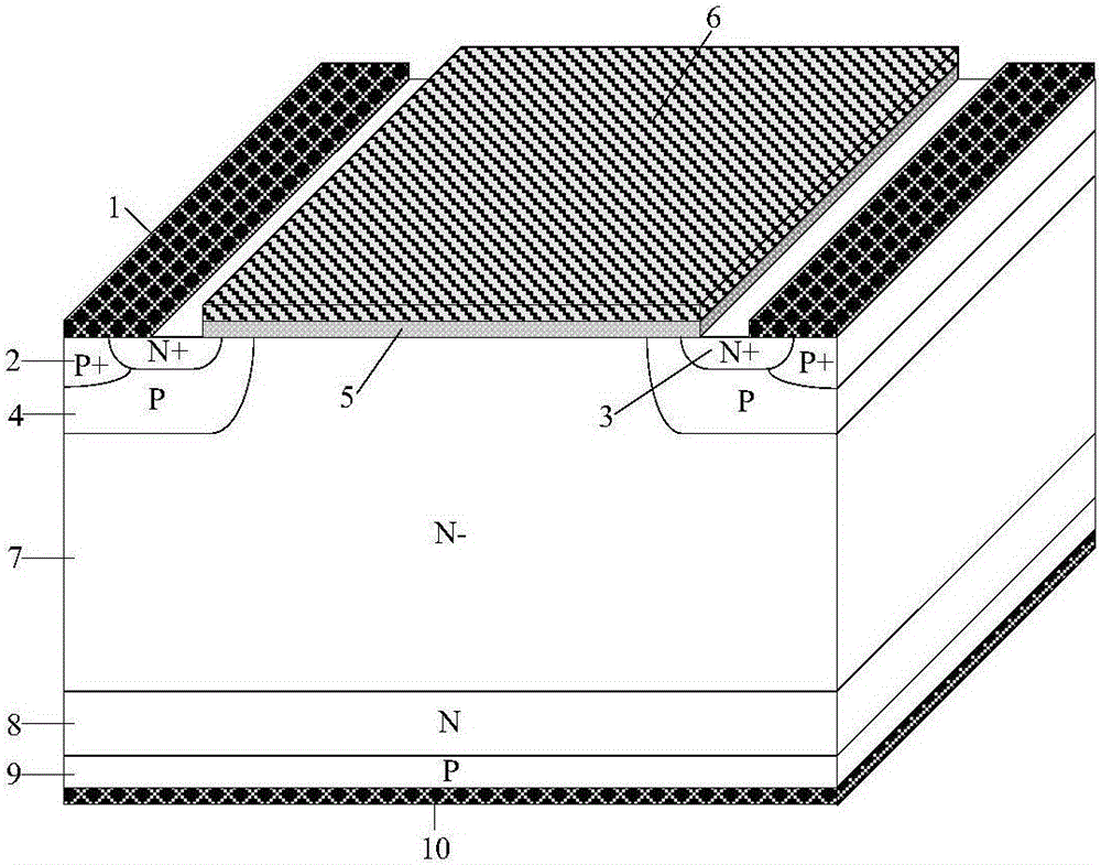
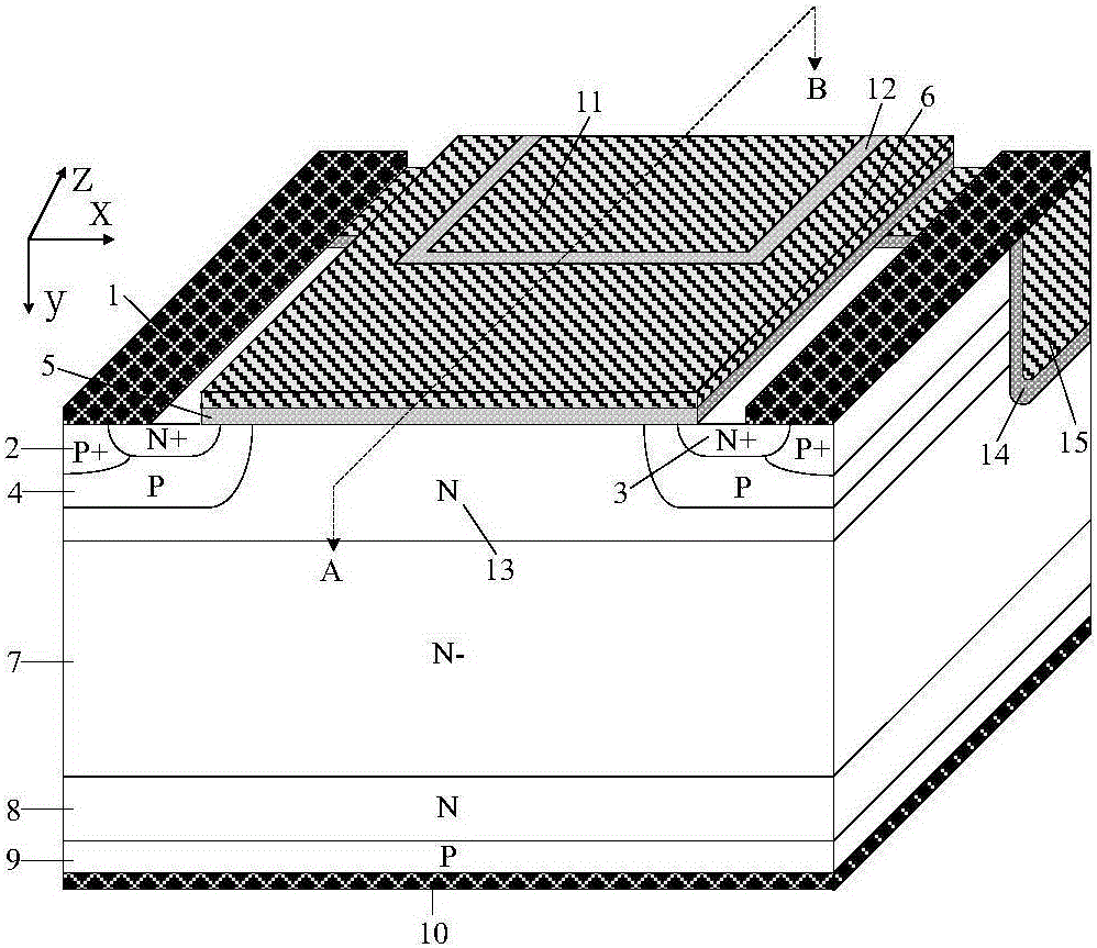
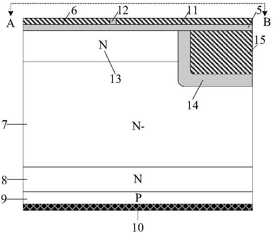
[0051] A planar gate IGBT, its semi-cellular structure and the section along the AB line are as follows figure 2 and image 3As shown, it includes: the back collector metal 10, the P-type collector region 9, the N-type field stop layer 8 and the N-drift region 7 are stacked sequentially from bottom to top; it is characterized in that the upper layer of the N-drift region 7 There is also an N-type layer 13, the doping concentration of the N-type layer 13 is greater than the doping concentration of the N-drift region 7; the two sides of the upper layer of the N-type layer 13 have a p-type base region 4, and the p-type base region 4. The upper layer has mutually independent N+ emitter regions 3 and P+ emitter regions 2; the N-type layer 13 on one side along the longitudinal direction also has a groove structure composed of a first dielectric layer 14 and a first electrode 15, the The depth of the trench structure is greater than the depth of the N-type layer 13 and penetrates t...

Embodiment 2

[0053] A planar gate IGBT, its semi-cellular structure and the section along the AB line are as follows Figure 4 and Figure 5 As shown, on the basis of Example 1, there is also a p-type buried layer with a width of 20-30 microns in the N-type layer 13 between the p-type base regions 4 parallel to the length direction of the MOS channel. Layer 16, the thickness of the p-type buried layer 16 is less than the thickness of the p-type base region 4; in the direction perpendicular to the length of the MOS channel, the p-type buried layer 16 is located at the opposite end of the trench structure, and its width 1-5 microns. The existence of the p-type buried layer 16 has further shielded the influence of the n-type layer 13 on the breakdown voltage of the device, and a high concentration of the n-type layer 13 can be used; simultaneously, the existence of the p-type buried layer 16 also affects the second dielectric layer 5 on its top. It has the function of electric field shieldi...

Embodiment 3

[0055] A plane gate IGBT, its section along the AB line is as follows Figure 6 As shown, on the basis of Embodiment 2, the p-type buried layer 16 is discontinuous and evenly distributed in the n-type layer 13 in the direction perpendicular to the length of the MOS channel. The discontinuous and evenly distributed p-type buried layer 16 can provide better electric field shielding effect and reduce the negative impact on conduction characteristics.


PUM


Abstract

The invention belongs to the technical field of a power semiconductor device, and relates to a plane gate IGBT and a manufacturing method therefor. On the basis of the conventional plane gate IGBT device structure, a surface recombination device structure is introduced, so that the gate electrode capacitance, particularly the gate electrode-collector electrode capacitance of the device is reduced, the switching speed of the device is improved, and the switching loss of the device is lowered; and meanwhile, the forward conduction voltage drop and the drift region carrier concentration distribution of the device are improved, the performance of the device is enhanced, and degradation of the blocking performance of the device is prevented.

Description

technical field [0001] The invention belongs to the technical field of power semiconductor devices, and relates to an insulated gate bipolar transistor (IGBT), in particular to a planar gate insulated gate bipolar transistor. Background technique [0002] Insulated Gate Bipolar Transistor (IGBT) is a new type of power electronic device combining MOS field effect and bipolar transistor. It not only has the advantages of easy driving and simple control of MOSFET, but also has the advantages of low conduction voltage of power transistor, large on-state current and small loss. It has become one of the core electronic components in modern power electronic circuits and is widely used in Various fields of the national economy such as communications, energy, transportation, industry, medicine, household appliances and aerospace. The application of IGBT plays an extremely important role in improving the performance of power electronic systems. [0003] Since the invention of IGBT, ...

Claims


Application Information

Patent Timeline
IPC IPC(8): H01L29/739H01L21/331H01L29/06H01L29/36H01L29/41
CPCH01L29/0684H01L29/36H01L29/41H01L29/66333H01L29/7398
Inventor 张金平陈文梅刘竞秀李泽宏任敏高巍张波
Owner UNIV OF ELECTRONIC SCI & TECH OF CHINA
Why Eureka
Try Eureka