Texturing method for diamond wire-cut polycrystalline silicon wafers

A diamond wire cutting, polycrystalline silicon wafer technology, applied in chemical instruments and methods, crystal growth, photovoltaic power generation and other directions, can solve the problems that the morphology of the damaged layer cannot be flexibly controlled, and it is difficult to form a smaller and more uniform suede, etc. Low reflectivity and uniform suede effect

Active Publication Date: 2017-08-01
云南合义德新材料有限公司
View PDF4 Cites 3 Cited by
  • Summary
  • Abstract
  • Description
  • Claims
  • Application Information

AI Technical Summary

Problems solved by technology

Mortar multi-wire cutting of silicon wafers is affected by the slicing process, so the morphology of the damaged layer cannot be flexibly controlled, and it is difficult to form a smaller and more uniform suede surface

Method used


Image

  • Texturing method for diamond wire-cut polycrystalline silicon wafers
  • Texturing method for diamond wire-cut polycrystalline silicon wafers
  • Texturing method for diamond wire-cut polycrystalline silicon wafers

Examples


Embodiment 2

[0041] Embodiment 2 The inventive method

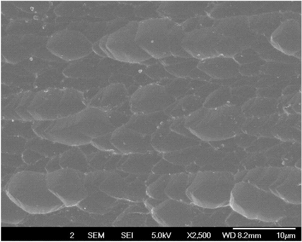
[0042] 1) Take the polycrystalline silicon wafer after diamond wire cutting, and grind the surface of the polycrystalline silicon wafer. The grinding liquid used for grinding is composed of 280 mesh silicon carbide and a dispersant in a mass ratio of 1:1. The dispersant is produced by Beijing Hedefeng Material Technology Co., Ltd. The commercially available dispersant is HMC-430DC, the pressure of the grinding head is 0.2MPa, and the surface of the polycrystalline silicon wafer is ground for 20s. After grinding, the surface roughness of the polycrystalline silicon wafer is 1.5um, and the depth of the damaged layer is 3um. Spray and clean the surface of the polysilicon wafer for 60s to remove the polishing liquid on the surface of the polysilicon wafer;

[0043] 2) Immerse the polysilicon wafer treated in 1) completely in the acidic texturing solution for 120s. The temperature of the texturing solution is 8°C to form a textured surface...

Embodiment 3

[0049] Embodiment 3 The inventive method

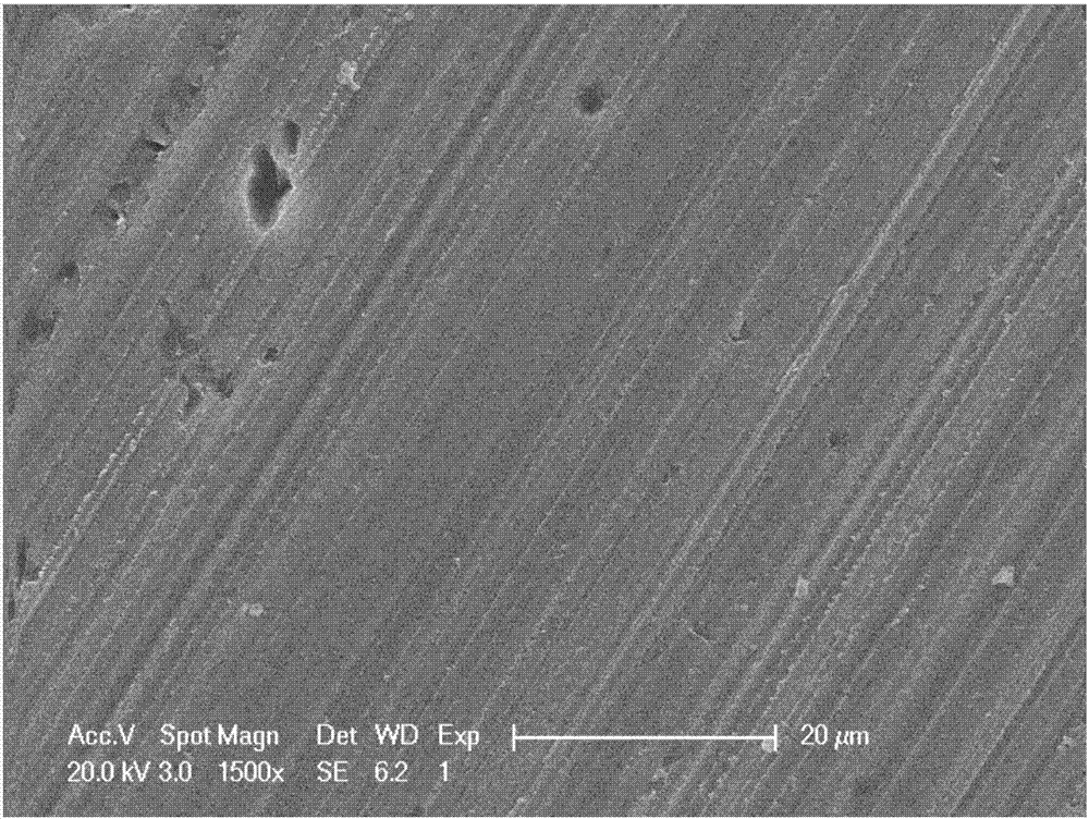
[0050] 1) Take the polysilicon wafer after diamond wire cutting, and grind the surface of the polysilicon wafer. The grinding liquid used for grinding is composed of abrasive and dispersant in a mass ratio of 1:1. The abrasive is 400 mesh silicon carbide, and the dispersant is Beijing Hedefeng Material Technology Co., Ltd. Co., Ltd. produced and marketed a dispersant of the type HMC-430DC. The pressure of the grinding head was 0.3 MPa. The surface of the polysilicon wafer was ground for 20 seconds. After grinding, the surface roughness of the polysilicon wafer was 1um, and the depth of the damaged layer was 2um. Spray and clean the surface of the polysilicon wafer with deionized water for 60 seconds to remove the polishing liquid on the surface of the polysilicon wafer;

[0051] 2) Immerse the polysilicon wafer treated in 1) completely in the acidic texturing solution for 105s. The temperature of the texturing solution is 8°C to form ...

Embodiment 4

[0057] Embodiment 4 The inventive method

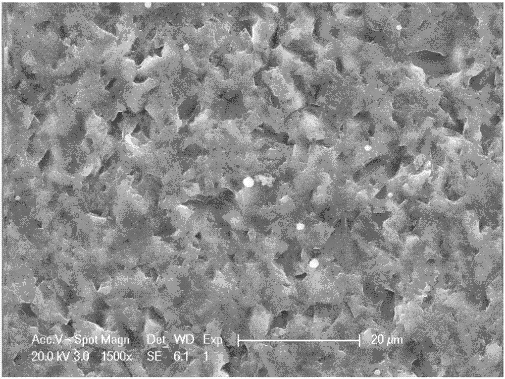
[0058] 1) Take the polycrystalline silicon wafer after diamond wire cutting, and grind the surface of the polycrystalline silicon wafer. The grinding liquid used in the grinding is composed of abrasive and dispersant in a mass ratio of 1:1. The abrasive is 800 mesh silicon carbide, and the dispersant is Beijing Hedefeng. The model of HMC-430DC dispersant produced and marketed by Material Technology Co., Ltd., the pressure of the grinding head is 0.4MPa, and the surface of the polycrystalline silicon wafer is ground for 10 seconds. After grinding, the surface roughness of the polycrystalline silicon wafer is 0.8um, and the depth of the damaged layer is 1.6um. , Spray and clean the surface of the polysilicon wafer with 25°C deionized water for 60 seconds to remove the polishing liquid on the surface of the polysilicon wafer;

[0059] 2) Immerse the polycrystalline silicon wafer treated in 1) completely in the acidic texturing solution f...


PUM

PropertyMeasurementUnit
reflectanceaaaaaaaaaa

Abstract

The invention relates to a texturing method of a polycrystalline silicon wafer cut by a diamond wire. The method comprises the following steps: getting a polycrystalline silicon wafer obtained after diamond wire cutting; carrying out preprocessing on the surface of the polycrystalline silicon wafer through grinding or abrasive blasting to fully eliminate cutting lines in the surface of the polycrystalline silicon wafer, and meanwhile, to make an appropriate damage layer on the surface of the polycrystalline silicon wafer; carrying out water washing on the polycrystalline silicon wafer obtained after processing, and placing the washed polycrystalline silicon wafer to acidic texturing liquid to form a textured surface; and carrying out water washing, alkaline washing, water washing, acid washing, water washing and drying in sequence on the polycrystalline silicon wafer obtained after texturing to finish texturing. The method can completely eliminate the cutting lines in the surface of the polycrystalline silicon wafer obtained after being cut by the diamond wire; and the shape of the damage layer on the surface of the polycrystalline silicon wafer can be controlled flexibly by controlling grinding or abrasive blasting parameters to enable the textured surface of the polycrystalline silicon wafer obtained after texturing to be more uniform and lower in reflection rate.

Description

technical field [0001] The invention relates to a method for making texture of a diamond wire-cut polycrystalline silicon wafer, which belongs to the field of solar cell manufacturing. Background technique [0002] At present, the cutting of polysilicon wafers in the photovoltaic field mainly adopts the mortar multi-wire cutting technology, but this technology has problems such as low cutting efficiency, high processing cost, and large pollution of waste mortar discharge. In contrast, the solid abrasive diamond wire saw cutting (referred to as diamond wire cutting) technology has the advantages of high cutting efficiency, low processing cost and low environmental pollution, and has received more and more attention. The future direction of slicing technology. [0003] Since the cutting principle of diamond wire dicing is different from that of mortar multi-wire dicing, there are great differences in the surface morphology of silicon wafers obtained by the two cutting process...

Claims


Application Information

Patent Timeline
Patent Type & Authority Patents(China)
IPC IPC(8): H01L31/0236C30B33/10
CPCY02E10/50
Inventor 雷深皓杜雪峰华永云
Owner 云南合义德新材料有限公司
Why Eureka
Try Eureka