Method for preparing photonic crystal structure LED based on 3D printing

A photonic crystal and 3D printing technology, applied in semiconductor devices, electrical components, circuits, etc., can solve the problems of complex realization methods of photonic crystal nanopatterns, and achieve the effects of rich patterns, improved production efficiency, and simple preparation process.

Active Publication Date: 2018-08-31
TAIYUAN UNIV OF TECH
View PDF6 Cites 0 Cited by
  • Summary
  • Abstract
  • Description
  • Claims
  • Application Information

AI Technical Summary

Problems solved by technology

[0004] In order to solve the problem of complex realization methods of photonic crystal nano-patterns, the present invention provides a method for preparing photonic crystal structure LEDs based on 3D printing

Method used


Image

  • Method for preparing photonic crystal structure LED based on 3D printing
  • Method for preparing photonic crystal structure LED based on 3D printing
  • Method for preparing photonic crystal structure LED based on 3D printing

Examples


Embodiment Construction

[0033] A method for preparing a photonic crystal structure LED based on 3D printing, comprising the following steps:

[0034] Step 1: Select an epitaxial wafer grown by MOCVD or MBE with a nucleation layer, an unintentionally doped layer, an N-type layer, a multi-period quantum well active layer, and a P-type layer as the substrate;

[0035] Step 2: The epitaxial wafer is coated with photoresist, exposed, developed, etched, and cleaned to form an N-type mesa;

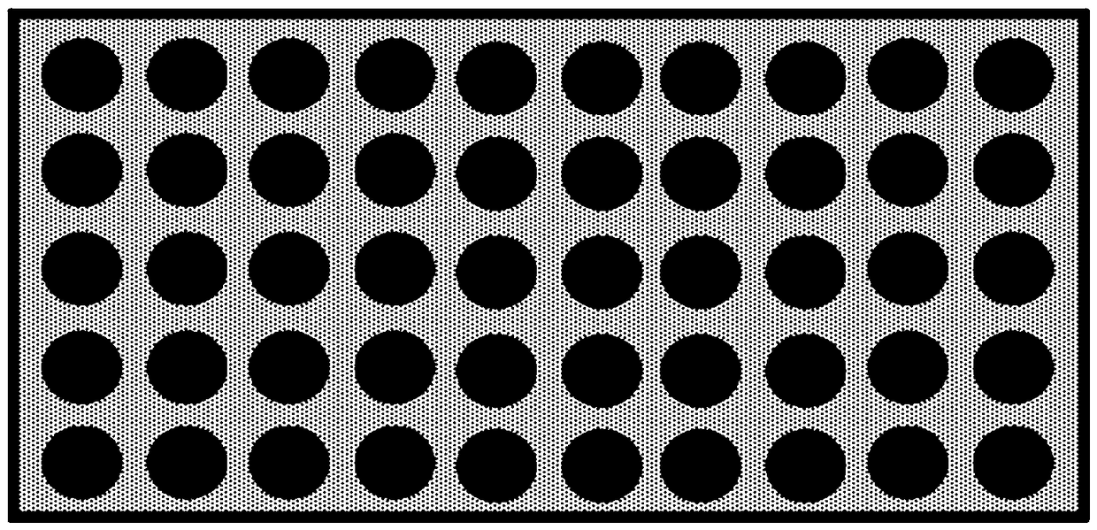
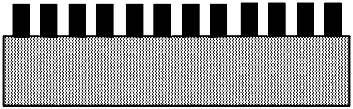
[0036] Step 3: Write the motion path program of 3D transparent conductive layer print head, 3D photonic crystal print head, 3D N-type electrode print head and 3DP-type electrode print head to meet the structural design requirements;

[0037] Step 4: Clean the epitaxial wafer and put it into the 3D printer as a substrate. Use a single or array 3D transparent conductive layer print head to print a transparent conductive layer on the P-type layer of the epitaxial wafer. The 3D printing method used is fusion or laser One o...


PUM


Abstract

The invention belongs to the field of optoelectronic devices and particularly relates to a method for preparing a photonic crystal structure LED based on 3D printing. The method comprises the steps of etching an n-type mesa on an epitaxial wafer with a low temperature nucleation layer, an unintentionally doped GaN layer, an N-type GaN layer, a multi-quantum well active layer and a P-type Gan layer, printing a thin transparent conductive layer on the n-type mesa, carrying out 3D printing of a photonic crystal on the transparent conductive layer, finally carrying out 3D printing of an n-type electrode on the n-type layer, and carrying out 3D printing of a p-type electrode on the transparent conductive layer which is not coated with the photonic crystal. According to the method, the 3D printing is used to prepare the photonic crystal structure LED, formed photonic crystal patterns are rich, the preparation process is simple, and the production efficiency can be improved.

Description

technical field [0001] The invention belongs to the field of optoelectronic devices, and in particular relates to a method for preparing a photonic crystal structure LED based on 3D printing. Background technique [0002] Light Emitting Diode (LED) has the characteristics of high brightness, low energy consumption, long life, fast response and environmental protection, and is widely used in indoor and street lighting, traffic signals and outdoor displays, automotive lighting, LCD backlight and many other fields. [0003] At present, the internal quantum efficiency of blue GaN-based LEDs can reach more than 80%, but the external quantum efficiency of high-power LED chips is usually only about 40%. The main factor restricting the improvement of external quantum efficiency is the low extraction efficiency of light caused by the total internal reflection of GaN interface and ITO interface and air interface. This is because the refractive index of GaN material is 2.5, the refrac...

Claims


Application Information

Patent Timeline
Patent Type & Authority Patents(China)
IPC IPC(8): H01L33/00B33Y10/00H01L33/36
CPCB33Y10/00H01L33/005H01L33/36H01L2933/0016
Inventor 卢太平朱亚丹周小润许并社
Owner TAIYUAN UNIV OF TECH
Why Eureka
Try Eureka