UV-visible absorption detection system based on micro-fluidic chip and detection method thereof

A microfluidic chip and detection system technology, applied in the field of detection systems, can solve problems such as difficult to achieve long optical path detection, increase the difficulty of chip processing, increase the amount of detection samples, etc., to reduce the amount of samples, low detection cost, Versatile effect

Inactive Publication Date: 2016-09-28
SUZHOU WENHAO MICROFLUIDIC TECH CO LTD
View PDF15 Cites 9 Cited by
  • Summary
  • Abstract
  • Description
  • Claims
  • Application Information

AI Technical Summary

Problems solved by technology

Among them, laser-induced fluorescence detection has high sensitivity and is suitable for the detection of various substances in chip microchannels. However, many substances have no fluorescent properties and require fluorescent labeling. In many experiments, it is impossible to ensure whether the properties of the tested substances after labeling Changes will directly affect the reliability of the experimental results, and the application is limited. The interface between the mass spectrometer detector and the microfluidic chip is difficult. In comparison, the ultraviolet-visible absorption detection operation unit is simple, the detection cost is low, and the versatility Strong, if it is integrated into a microfluidic chip, it can realize portable detection, which is of great significance to the detection of heavy metals or small molecules in environmental water or food fields.
[0004] The principle of ultraviolet-visible absorption is Lambert-Beer's law, and the absorbance is proportional to the absorption path. For high-concentration samples, a chip with an ordinary size can meet the detection requirements, but for low-concentration samples, it is necessary to design and manufacture a chip with a long pathlength. This increases the processing difficulty of the chip and increases the amount of detection samples. It can be seen that it is difficult to achieve long optical path detection in the direction perpendicular to the chip channel.
In addition, commonly used chip materials such as glass and plastic have a large absorption of ultraviolet light and are not suitable for ultraviolet detection, while chip materials such as quartz and PDMS have little ultraviolet absorption and are ideal materials for ultraviolet absorption photometric detection.

Method used


Image

  • UV-visible absorption detection system based on micro-fluidic chip and detection method thereof

Examples


Embodiment Construction

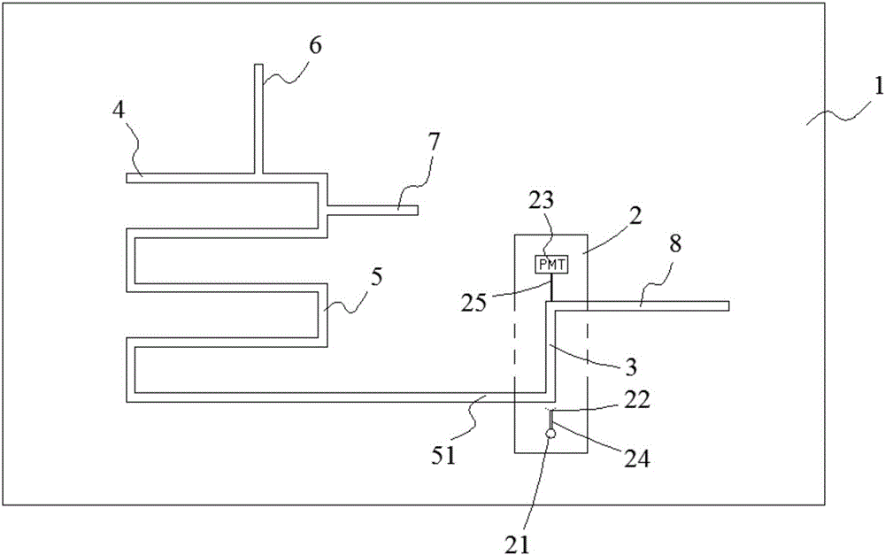
[0027] The purpose of the present invention is to provide a microfluidic chip system with ultraviolet-visible absorption detection function. The system injects a solution into the microfluidic chip under the action of an external driving force to process a microfluidic chip with a mixed detection microchannel structure. The chip is used as the carrier to realize the color reaction operation between the sample and the chromogen, and then, the ultraviolet-visible absorption long-path detection is carried out along the horizontal direction of the detection channel. This system can realize the portable quantitative detection of the content of ions or small molecules in the sample.

[0028] The technical solutions in the embodiments of the present invention will be described in detail below in conjunction with the accompanying drawings in the embodiments of the present invention. Obviously, the described embodiments are only some of the embodiments of the present invention, not all o...


PUM

PropertyMeasurementUnit
lengthaaaaaaaaaa

Abstract

The application discloses a UV-visible absorption detection system based on a micro-fluidic chip and a detection method thereof. The UV-visible absorption detection system comprises a chip substrate, a micro-channel formed on the chip substrate and a UV absorption detector integrated on the chip substrate, wherein the micro-channel comprises a detection channel, and rays generated by the UV absorption detector are parallel to the extending direction of the detection channel. A light source of the UV absorption detector emits in and out in the horizontal direction of the chip, namely, in the direction parallel to the channel of the chip, so that the problem of short absorption optical path is solved; a UV-visible absorption detection operation unit is simple, low in detection cost and strong in university; the UV-visible absorption detector is integrated into the micro-fluidic chip, so that detection convenience is realized, and the quantity of the consumed solution can reach several or dozens of micro-liters. Compared with a traditional UV-visible absorption detection system, the detection method provided by the invention is greatly lowered in sample consumption, and has significance on detection of ions, micromolecules and the like in the field of environmental water or food.

Description

technical field [0001] The application belongs to the field of microfluidic chip laboratory detection, and in particular relates to a detection system integrating an ultraviolet-visible absorber into a microfluidic chip, which can be used for ion or small molecule detection in the environment or food fields. Background technique [0002] Microfluidic chip laboratory (Lab on Chip) or Micro Total Analysis System (Micro Total Analysis System, or microTAS) refers to the basic A technology in which operating units are integrated or basically integrated on a chip of several square centimeters to complete different biological or chemical reaction processes and analyze their products. It achieves chemical analysis and detection through the intersection of analytical chemistry, micro-electromechanical processing (MEMS), computer, electronics, material science and biology, medicine and engineering, that is, to realize the overall miniaturization, automation, and integration from sampl...

Claims


Application Information

Patent Timeline
Patent Type & Authority Applications(China)
IPC IPC(8): G01N21/31G01N21/33B01L3/00
CPCB01L3/5027G01N21/31G01N21/33G01N2021/3133
Inventor 刘珊珊顾志鹏姚纪文聂富强
Owner SUZHOU WENHAO MICROFLUIDIC TECH CO LTD
Why Eureka
Try Eureka