A kind of method of monoatomic layer deposition technology to grow Ni-containing thin film

A single atomic layer technology, applied in the coating, metal material coating process, gaseous chemical plating, etc., can solve the problems such as the difficulty of forming the Ni silicide deposition layer and the inability of metal silicide to meet the demand, and achieve volatility Good, low cost, high thermal decomposition temperature effect

Active Publication Date: 2018-10-16
INST OF MICROELECTRONICS CHINESE ACAD OF SCI +1
View PDF2 Cites 0 Cited by
  • Summary
  • Abstract
  • Description
  • Claims
  • Application Information

AI Technical Summary

Problems solved by technology

In this case, the traditional PVD method to deposit Ni to form metal silicide can no longer meet the demand
Especially when the silicon material in the source and drain regions is Fin or nanowires, the Ni silicide deposition layer deposited by PVD method is difficult to form

Method used


Image

  • A kind of method of monoatomic layer deposition technology to grow Ni-containing thin film
  • A kind of method of monoatomic layer deposition technology to grow Ni-containing thin film
  • A kind of method of monoatomic layer deposition technology to grow Ni-containing thin film

Examples


Embodiment 1

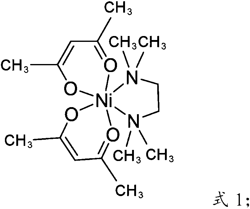
[0051] A Ni(acac) 2 (TMEDA) is Ni source, with N 2 h 4 Be the Ni thin film atomic layer deposition method of reducing agent, comprise following process:

[0052] 1) With Si as the substrate, the deposition temperature is 250°C, Ni source Ni(acac) 2 The heating temperature of (TMEDA) is 90°C to vaporize it, and high-purity nitrogen is used as the carrier gas, and the gas phase Ni source Ni(acac) is passed into it. 2 (TMEDA), the carrier gas flow rate is 20 sccm. The pulse time is 12s, and the waiting time is 10s;

[0053] 2) Use high-purity nitrogen to clean after completing a pulse, and the cleaning time is 25s;

[0054] 3) Reducing agent N 2 h 4 The heating temperature is 60°C to vaporize it, using high-purity nitrogen as the carrier gas, the flow rate of the carrier gas is 60 sccm, and N is introduced in pulse form. 2 h 4 . The pulse time is 5s, and the waiting time is 15s;

[0055] 4) Use high-purity nitrogen to clean after completing a reducing agent pulse, and ...

Embodiment 2

[0059] A Ni(acac) 2 (TMEDA) is Ni source, with Me 2 NH·BH 3 Be the Ni thin film atomic layer deposition method of reducing agent, comprise following process:

[0060] 1) with SiO 2 As the substrate, the deposition temperature is 300°C, the Ni source Ni(acac) 2 The heating temperature of (TMEDA) is 150°C to vaporize it, and high-purity argon is used as the carrier gas, and the gas phase Ni source Ni(acac) is passed into it. 2 (TMEDA), the carrier gas flow rate is 90 sccm. The pulse time is 5s, and the waiting time is 20s;

[0061] 2) After completing a pulse, use high-purity argon to clean, and the cleaning time is 45s;

[0062] 3) Reductant Me 2 NH·BH 3 The heating temperature is 90°C to vaporize it, using high-purity argon as the carrier gas, the flow rate of the carrier gas is 10 sccm, and the Me 2 NH·BH 3 . The pulse time is 15s, and the waiting time is 5s;

[0063] 4) Use high-purity nitrogen to clean after completing a reducing agent pulse, and the cleaning ti...

Embodiment 3

[0066] A Ni(acac) 2 (TMEDA) as Ni source, with CH 3 OH is the Ni thin film atomic layer deposition method of reducing agent, comprises following process:

[0067]1) With silicon nitride as the substrate, the deposition temperature is 350°C, Ni source Ni(acac) 2 The heating temperature of (TMEDA) is 120°C to vaporize it, and high-purity argon is used as the carrier gas, and the gas phase Ni source Ni(acac) is passed into it. 2 (TMEDA), the carrier gas flow rate is 120 sccm. The pulse time is 8s, and the waiting time is 5s;

[0068] 2) After completing a pulse, use high-purity argon to clean, and the cleaning time is 15s;

[0069] 3) Reductant CH 3 The heating temperature of OH is 25°C to vaporize it, using high-purity argon as the carrier gas, the flow rate of the carrier gas is 160 sccm, and CH is introduced in the form of pulses 3 Oh. The pulse time is 20s, and the waiting time is 10s;

[0070] 4) Use high-purity nitrogen to clean after completing a reducing agent pul...


PUM

PropertyMeasurementUnit
electrical resistivityaaaaaaaaaa
thicknessaaaaaaaaaa
electrical resistivityaaaaaaaaaa

Abstract

The invention provides a method for growing a Ni-containing film by monoatomic layer deposition, comprising the following steps: A) placing a substrate in a reaction chamber, and feeding a gaseous Ni source into the reaction chamber in pulse form under vacuum conditions Depositing is carried out to obtain a substrate deposited with a Ni source, and the Ni source includes a compound having a structure shown in formula I; B) passing a gas phase reducing agent into the reaction chamber in a pulsed form, and performing a process on the Ni source deposited on the substrate Reduction, to obtain a substrate deposited with a Ni film. The present invention adopts the Ni source with the structure of formula I, and applies it in atomic layer deposition (ALD), so that a Ni-containing deposition layer with better shape retention can be deposited on a nanoscale semiconductor device. Moreover, the resistivity of the Ni film prepared by the method of the present invention is lower, and the experimental results show that the resistivity of the Ni film prepared by the present invention is 13-24 μΩ·cm.

Description

technical field [0001] The invention belongs to the technical field of semiconductor preparation, and in particular relates to a method for growing a Ni-containing thin film by monoatomic layer deposition technology. Background technique [0002] Ni metal silicide is widely used as a contact material in CMOS (complementary metal oxide semiconductor) device source and drain technology. As a contact metal, Ni-silicide has outstanding advantages such as low resistivity, continuity and uniformity. In traditional Ni silicide, a layer of Ni metal is deposited by PVD (Physical Vapor Deposition, physical vapor deposition) technology, and then Ni and silicon are reacted to form silicide through thermal annealing. [0003] Due to the development of microelectronics and deep submicron chip technology, the size of devices and materials is continuously reduced, and the aspect ratio of devices is continuously increased, so the thickness of the materials used is reduced to the order of se...

Claims


Application Information

Patent Timeline
Patent Type & Authority Patents(China)
IPC IPC(8): C23C16/18C23C16/455H01L21/02
CPCC23C16/18C23C16/45527H01L21/02697C23C16/45553H01L21/28518H01L21/28562C23C16/45525H01L21/28556H01L21/76879
Inventor 丁玉强杜立永张羽翔赵超项金娟
Owner INST OF MICROELECTRONICS CHINESE ACAD OF SCI
Why Eureka
Try Eureka