All-semiconductor mid-infrared tunable absorber
A semiconductor and absorber technology, which is applied in the field of all-semiconductor mid-infrared frequency-tunable absorbers, achieves the effects of simple structure, changing optical response, and enriching implementation means
- Summary
- Abstract
- Description
- Claims
- Application Information
AI Technical Summary
Problems solved by technology
Method used
Image
Examples
no. 1 example
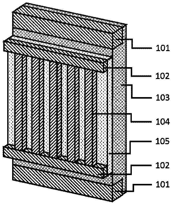
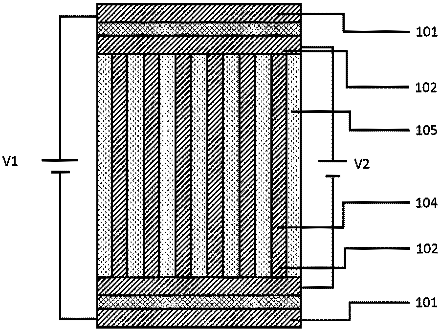
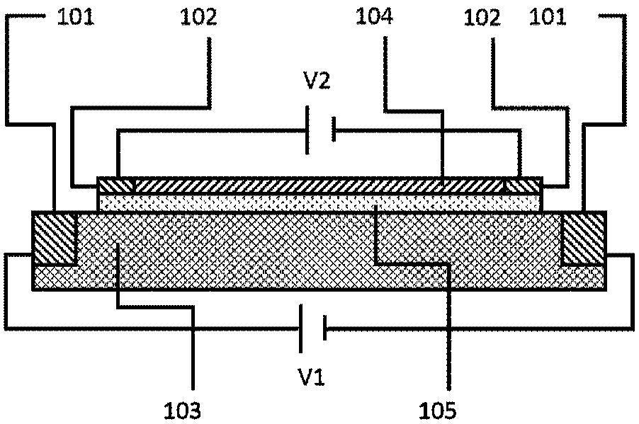
[0026] see Figure 1 to Figure 3 As shown, the present invention provides an all-semiconductor mid-infrared tunable frequency absorber, comprising:
[0027] An n / p-type doped semiconductor layer 103 is rectangular, and the thickness of the n / p-type doped semiconductor layer 103 is greater than the tunneling depth of light waves in the working band of the absorber. It is used as a reflector, and the n / p-type The material of the p-type doped semiconductor layer 103 is a semiconductor material that realizes metallicity through doping, and the n / p-type doped semiconductor layer 103 described in the first embodiment is an n-type doped semiconductor material (InAs) with a thickness greater than 1 micron;
[0028] Two first bias voltage control parts 101, which are formed at opposite ends of the n / p-type doped semiconductor layer 103;
[0029] An intrinsic semiconductor dielectric isolation layer 105, which is fabricated on the n / p type doped semiconductor layer 103, the length of ...
no. 2 example
[0036] see Figure 5 to Figure 7 As shown, the present invention provides an all-semiconductor mid-infrared broadband frequency-tunable absorber. The structure of the second embodiment of the present invention is basically the same as that of the first embodiment, except that the n / p type doped semiconductor grating strips 104 are in groups of two, and the width of one strip in each group is less than the width of another (see Image 6 ), the strip widths are 190-210 nanometers and 390-410 nanometers respectively, and the grating period is 2 microns; the thickness of the intrinsic semiconductor dielectric isolation layer 105 is 330-350 nanometers.
[0037] Figure 8 The doping concentration of the n-type doped semiconductor layer (InAs) and the n-type doped semiconductor compound grating layer (InAs) of this all-semiconductor mid-infrared broadband tunable frequency absorber in the second embodiment of the present invention is N= Absorption lines at 7E19 and N=9E19.
[003...
PUM
 Abstract
Description
Claims
Application Information


