Pixel circuit, driving method thereof, display panel and display apparatus

A pixel circuit and level technology, applied to static indicators, instruments, etc., can solve the problems of current weakening, voltage reduction, OLED display unevenness, etc., and achieve the effect of avoiding hysteresis effect and weakening voltage drop

Active Publication Date: 2016-10-12
WUHAN TIANMA MICRO ELECTRONICS CO LTD +1
View PDF5 Cites 20 Cited by
  • Summary
  • Abstract
  • Description
  • Claims
  • Application Information

AI Technical Summary

Problems solved by technology

In the prior art, usually one or more columns of pixel circuits share a first power supply voltage VDD. Due to the voltage division effect of the circuit traces, a voltage drop occurs during the transmission of the first power supply voltage VDD to the anode of the organic light emitting diode D1. 1. The problem of current weakening. Since the length of the traces from the first power supply voltage VDD to each pixel circuit is not exactly the same, the degree of the voltage reduction of the first power supply voltage VDD and the current weakening are not completely the same, resulting in uneven display of the OLED display. The phenomenon

Method used


Image

  • Pixel circuit, driving method thereof, display panel and display apparatus
  • Pixel circuit, driving method thereof, display panel and display apparatus
  • Pixel circuit, driving method thereof, display panel and display apparatus

Examples


Embodiment Construction

[0017] In order to make the above objects, features and advantages of the present invention more comprehensible, the present invention will be further described below in conjunction with the accompanying drawings and embodiments.

[0018] It should be noted that in the following description, specific details are set forth in order to fully understand the present invention. However, the present invention can be implemented in many other ways than those described here, and those skilled in the art can make similar extensions without departing from the connotation of the present invention. Accordingly, the present invention is not limited to the specific embodiments disclosed below.

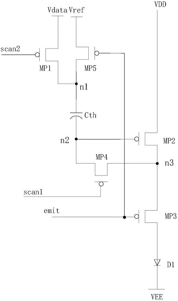
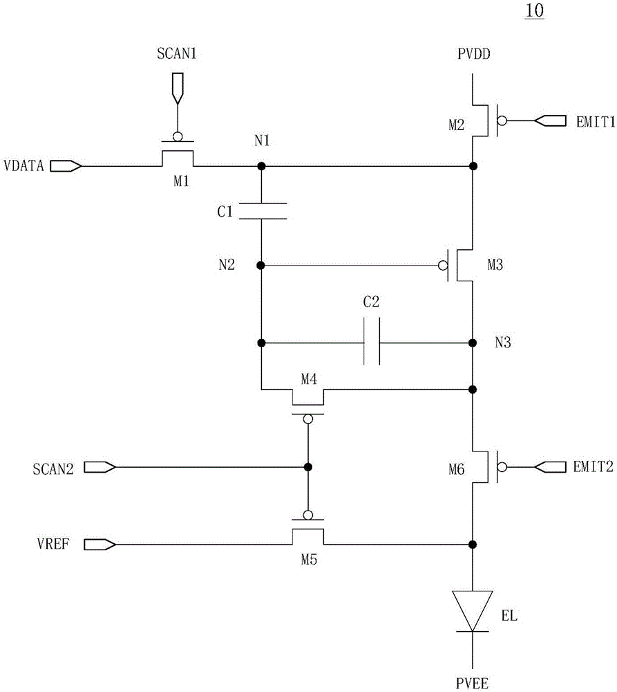
[0019] Please refer to image 3 , image 3 It is a schematic structural diagram of a pixel circuit provided by an embodiment of the present invention. Such as image 3 As shown, a pixel circuit 10 provided by an embodiment of the present invention includes: a first transistor M1, a second transi...


PUM


Abstract

The invention describes a pixel circuit, a driving method thereof, a display panel and a display apparatus. The pixel circuit comprises a first transistor to a sixth transistor, a first capacitor, a second capacitor and a light emitting element, wherein the first transistor transmits data signals to a first node, the second transistor transmits first power source signals to the first node, the third transistor transmits the electric signals from the second transistor to a third node, a fourth transistor transmits the potential of the third node to a second node, the fifth transistor transmits referential voltage to the anode of the light emitting element, the sixth transistor transmits the potential of the third node to the anode of the light emitting element, the first capacitor couples the potentials of the first node and the second node, and the second capacitor couples the potentials of the second node and the third node. The light emitting unit in the pixel circuit may not emit light undesirably, and the threshold-voltage of the driving transistors can be captured accurately. Display consistency can be improved.

Description

technical field [0001] The present invention relates to the field of display technology, in particular to a pixel circuit and a driving method thereof, a display panel including the pixel circuit, and a display device. Background technique [0002] The organic light-emitting display adopts an organic light-emitting diode (Organic Light-Emitting Diode, OLED) as a light-emitting element, and has advantages such as self-illumination, high contrast ratio, ultra-wide viewing angle, and low power consumption. An OLED display generally includes a pixel array and a pixel circuit that provides driving current to each organic light emitting diode in the pixel array. [0003] Such as figure 1 Shown is a schematic structural diagram of a pixel circuit of an existing OLED display. The pixel circuit includes a first transistor MP1, a second transistor MP2, a third transistor MP3, a fourth transistor MP4, a fifth transistor MP5, a storage capacitor Cth and an organic light emitting diode...

Claims


Application Information

Patent Timeline
Patent Type & Authority Applications(China)
IPC IPC(8): G09G3/3208
CPCG09G3/3208
Inventor 吴桐邹文晖李玥钱栋刘刚朱仁远向东旭
Owner WUHAN TIANMA MICRO ELECTRONICS CO LTD
Why Eureka
Try Eureka