Low on-resistance lateral double-diffusion metal oxide semiconductor device
An oxide semiconductor and lateral double-diffusion technology, which is applied in semiconductor devices, electrical components, circuits, etc., can solve the problems that LDMOS withstand voltage and on-resistance cannot be optimized, and it is difficult to achieve low on-resistance LDMOS. Low on-resistance, reduced on-resistance, and low on-resistance effects
- Summary
- Abstract
- Description
- Claims
- Application Information
AI Technical Summary
Problems solved by technology
Method used
Image

Examples
Embodiment Construction
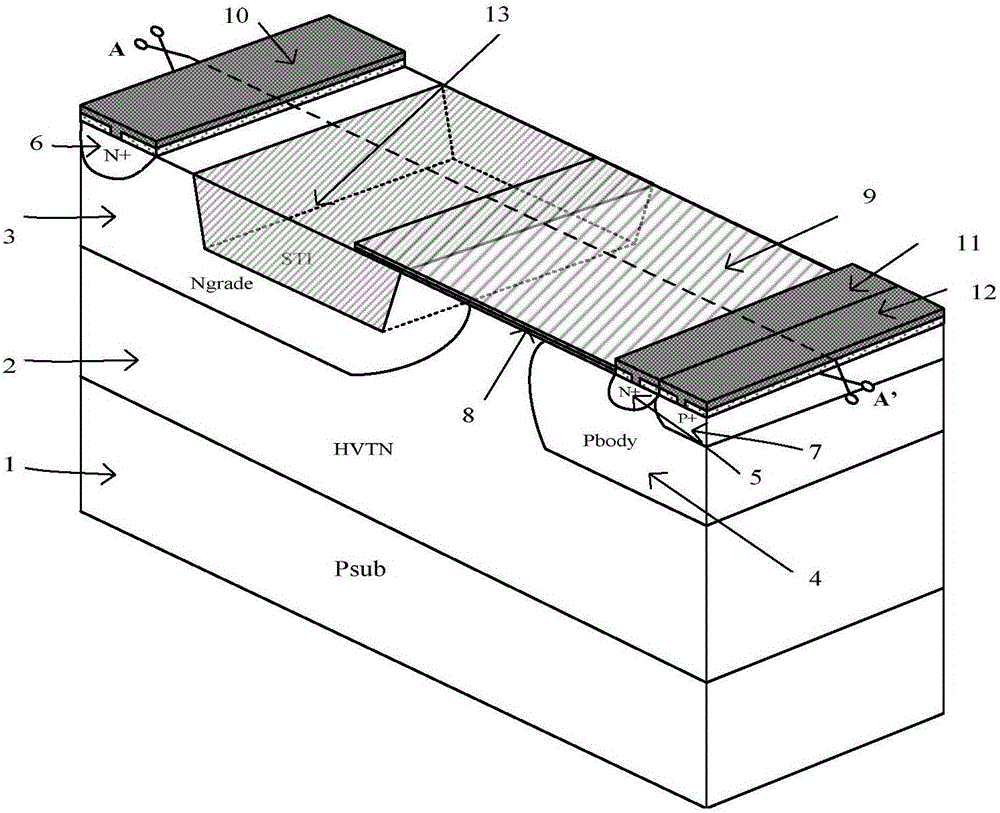
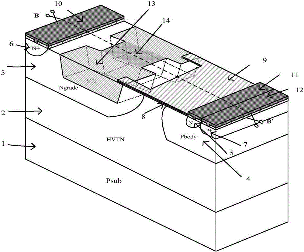
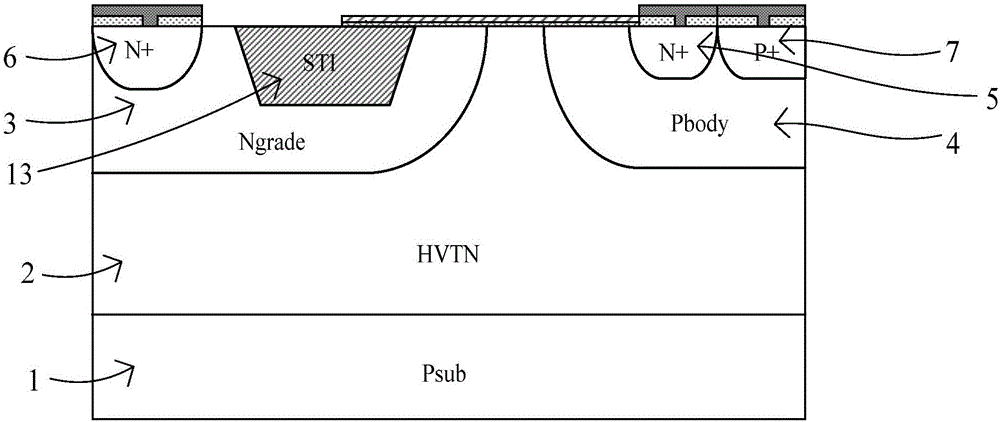
[0023] A low on-resistance lateral double-diffused metal oxide semiconductor device, comprising: a P-type substrate 1, a high-voltage N-type region 2 is arranged above the P-type substrate 1, and an N-type region is arranged above the high-voltage N-type region 2. Type drift region 3 and P-type body region, N-type drain region 6 and shallow trench isolation region are arranged in N-type drift region 3, N-type source region 5 and P-type region 7 are arranged in P-type body region 4, A gate oxide layer 8 is also provided above the high-voltage N-type region 2, and the two ends of the gate oxide layer 8 extend to the top of the P-type body region 4 and the top of the first shallow trench isolation region 13 respectively. 8 is provided with a polysilicon gate field plate 9, and a drain metal contact 10, a source metal contact 11 and a body metal contact 12 are respectively provided on the upper surfaces of the N-type drain region 6, the N-type source region 5 and the P-type region ...
PUM
 Abstract
Description
Claims
Application Information
 - Generate Ideas
- Intellectual Property
- Life Sciences
- Materials
- Tech Scout
- Unparalleled Data Quality
- Higher Quality Content
- 60% Fewer Hallucinations
Browse by: Latest US Patents, China's latest patents, Technical Efficacy Thesaurus, Application Domain, Technology Topic, Popular Technical Reports.
© 2025 PatSnap. All rights reserved.Legal|Privacy policy|Modern Slavery Act Transparency Statement|Sitemap|About US| Contact US: help@patsnap.com