Facet film-plating clamp for semiconductor laser chip

A semiconductor and laser technology, which is applied in the direction of semiconductor lasers, lasers, laser parts, etc., can solve the problems of less storage space for chips, complex fixture structure, and decreased precision, and achieve reduced manufacturing process steps, simple fixture components, and reduced shading area. small effect

Inactive Publication Date: 2016-10-12
XIAN LIXIN PHOTOELECTRIC SCI & TECH
View PDF7 Cites 8 Cited by
  • Summary
  • Abstract
  • Description
  • Claims
  • Application Information

AI Technical Summary

Problems solved by technology

[0006] 1. The complex structure of the fixture is not conducive to processing and cleaning and maintenance after use, resulting in rapid decline in accuracy and shortened service life
[0007] 2. At present, many fixtures can only be coated on one side, and double-sided coating needs to be disassembled and assembled twice. Repeated operations will cause great damage to the chip, and the large angle of the fixed area will cause shadows;
[0008] 3. The structure of the chip is complex, the tolerance is small, and the requirements for personnel skills are high. If the stacking is not smooth during the operation process, it will easily cause contamination or damage to the cavity surface, resulting in low work efficiency, low yield, and damage to the product;
[0009] 4. Unreasonable structural design of individual fixtures, chip clamping is not firm, slides or falls, which will cause damage;
[0010] 5. The fixture structure is complex, there are many parts, the precision of the fixture is high, the processing yield is low, and the processing cost is high;
[0011] 6. There are many fixture assemblies, fewer places to store chips, less amount of coating at one time, and high production costs; the fixture structure is complex and difficult to clean, and it is easy to contaminate the end face of the chip during the coating process

Method used


Image

  • Facet film-plating clamp for semiconductor laser chip
  • Facet film-plating clamp for semiconductor laser chip
  • Facet film-plating clamp for semiconductor laser chip

Examples


Embodiment Construction

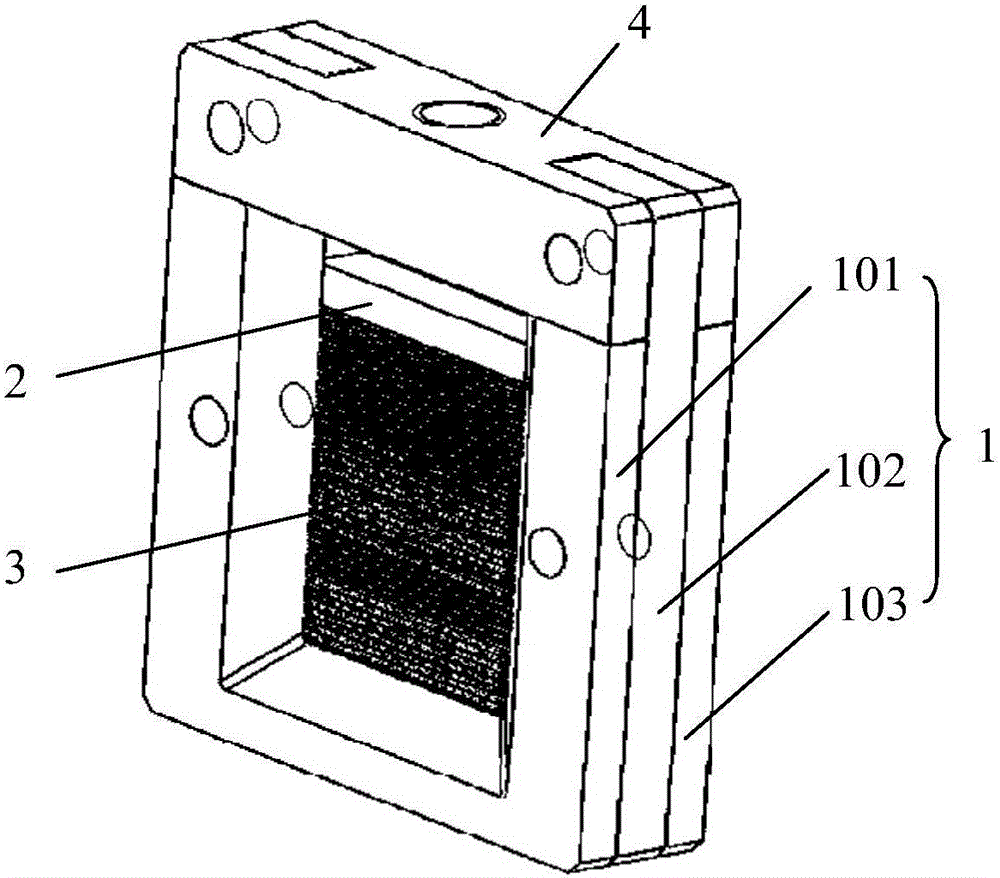
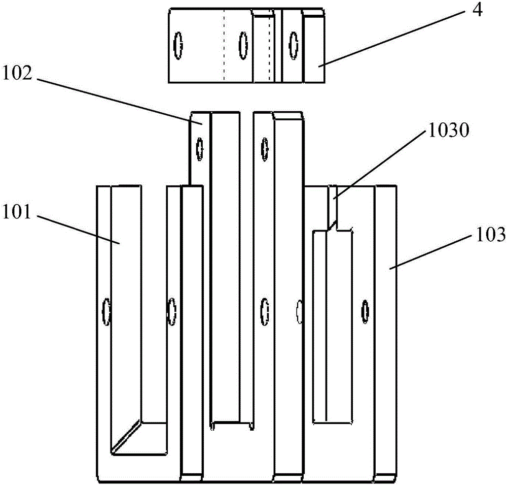
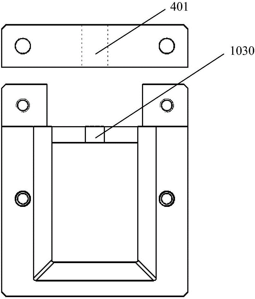
[0036] Such as figure 1 , figure 2 As shown, the coating fixture includes a flat U-shaped frame assembly 1 and a plug assembly located at the U-shaped open end (only the top wire fixing block 4 is shown in the figure), and is surrounded by the flat U-shaped frame assembly and the plug assembly. In the closed area of ​​the plane, several bars 3 and the stainless steel pads 2 provided at both ends are stacked and arranged sequentially from the U-shaped closed end to the U-shaped open end.

[0037] The flat U-shaped frame assembly is mainly composed of a U-shaped upper plate 101, a U-shaped middle plate 102 and a closed-loop lower plate 103, which are stacked in sequence in the vertical direction and fixed through screws. The inner width of the U-shaped middle plate 102 is larger than The inner width of the closed-loop lower plate 103 and the U-shaped upper plate 101, wherein the side cavities at both ends of several bars are just supported on the rail surface left by the close...


PUM


Abstract

The invention proposes a new semiconductor laser chip cavity surface coating fixture, which has stable clamping, simple structure, convenient operation, easy processing, large-scale coating, and effectively improves the coating quality. The semiconductor laser chip cavity surface coating fixture includes a flat U-shaped frame assembly and a plug assembly located at the U-shaped opening end. In the plane closed area formed by the flat U-shaped frame assembly and the plug assembly, several bars are closed from the U shape. The ends are stacked and arranged in turn toward the U-shaped opening; the inner width of the U-shaped middle plate of the flat U-shaped frame assembly is larger than the inner width of the lower plate and the U-shaped upper plate, so that the side cavities at both ends of several bars are just supported by the lower plate. The rail surface reserved by the U-shaped upper plate is covered by the rail surface reserved by the U-shaped upper plate, and the U-shaped middle plate is limited in the horizontal direction. The plug assembly is from the U-shaped open end to the U-shaped closed end. The plurality of bars apply top-tight pressure.

Description

technical field [0001] The invention relates to a semiconductor laser chip cavity surface coating fixture. Background technique [0002] High-power semiconductor lasers have the advantages of all-solid-state, small size, light weight, long life, high efficiency, high reliability, and high metal-to-semiconductor laser absorption, so they are widely used in pumping sources of solid-state lasers, laser processing, and laser cutting. , precision detection and measurement, communication and information processing, medical treatment and beauty, military and other aspects, and has caused revolutionary breakthroughs in many fields, with huge market demand and development potential. [0003] Cleavage plane of resonator is an important part of semiconductor laser, and it has an important influence on the reliability of the device. Generally, the reflectivity of the natural cleavage plane of GaAs laser is about 32%, which is not ideal, and the natural cleavage plane is easy to oxidize...

Claims


Application Information

Patent Timeline
Patent Type & Authority Applications(China)
IPC IPC(8): H01S5/028
CPCH01S5/028
Inventor 王希敏吴建耀杨国文
Owner XIAN LIXIN PHOTOELECTRIC SCI & TECH
Why Eureka
Try Eureka