Preparation method of porous zinc oxide nanowire arrays
A nanowire array and porous zinc oxide technology, applied in the field of nanomaterials, can solve the problems of difficult recycling and small specific surface area, and achieve the effect of solving small specific surface area, improving specific surface area and excellent performance
- Summary
- Abstract
- Description
- Claims
- Application Information
AI Technical Summary
Problems solved by technology
Method used
Image
Examples
Embodiment 1
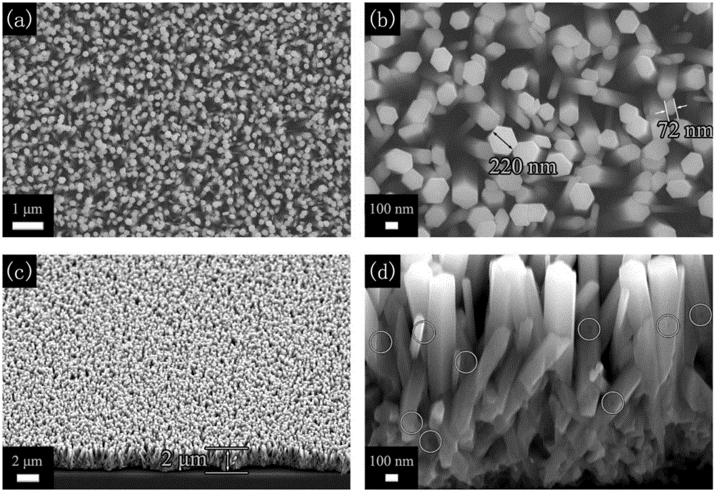
[0031] (1) Pretreatment of the substrate monocrystalline silicon wafer: Cut the monocrystalline silicon wafer substrate into a suitable shape, and perform ultrasonic cleaning with acetone, alcohol, and deionized water for 15 minutes in sequence.
[0032] (2) Preparation of zinc oxide seed layer: use the FJL-5600 ion beam surface treatment and irradiation simulation device to grow zinc oxide film on the pretreated single crystal silicon wafer by radio frequency sputtering as the zinc oxide seed layer, thin film The thickness is 10-30nm.
[0033] (3) Reaction solution preparation: configure ZnCl 2 Aqueous solution with a concentration of 0.2mol / L, after mixing evenly by magnetic stirring, add a certain amount of concentrated NH 3 ·H 2 O, the solution gradually becomes milky white, and the pH value of the reaction solution is 9.5 to 10.5 at this time, continue to stir until the solution is evenly mixed.
[0034] (4) Growth of porous zinc oxide nanowire array: transfer the reac...
Embodiment 2
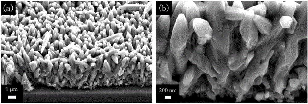
[0037] (1) Pretreatment of the substrate monocrystalline silicon wafer: Cut the monocrystalline silicon wafer substrate into a suitable shape, and perform ultrasonic cleaning with acetone, alcohol, and deionized water for 15 minutes in sequence.
[0038](2) Preparation of zinc oxide seed layer: use the FJL-5600 ion beam surface treatment and irradiation simulation device to grow zinc oxide film on the pretreated single crystal silicon wafer by radio frequency sputtering as the zinc oxide seed layer, thin film The thickness is 10-30nm.
[0039] (3) Reaction solution preparation: configure ZnCl 2 Aqueous solution with a concentration of 0.2mol / L, after mixing evenly by magnetic stirring, add a certain amount of concentrated NH 3 ·H 2 O, the solution gradually becomes milky white, and the pH value of the reaction solution is 9.5 to 10.5 at this time, continue to stir until the solution is evenly mixed.
[0040] (4) Growth of porous zinc oxide nanowire array: transfer the react...
Embodiment 3
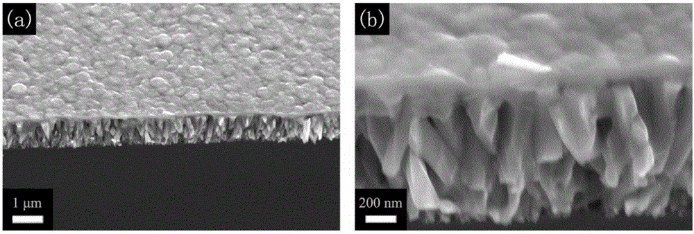
[0043] (1) Pretreatment of the substrate monocrystalline silicon wafer: Cut the monocrystalline silicon wafer substrate into a suitable shape, and perform ultrasonic cleaning with acetone, alcohol, and deionized water for 15 minutes in sequence.
[0044] (2) Preparation of zinc oxide seed layer: use the FJL-5600 ion beam surface treatment and irradiation simulation device to grow zinc oxide film on the pretreated single crystal silicon wafer by radio frequency sputtering as the zinc oxide seed layer, thin film The thickness is 10-30nm.
[0045] (3) Reaction solution preparation: configure ZnCl 2 Aqueous solution with a concentration of 0.2mol / L, after mixing evenly by magnetic stirring, add a certain amount of concentrated NH 3 ·H 2 O, the solution gradually becomes milky white, and the pH value of the reaction solution is 9.5 to 10.5 at this time, continue to stir until the solution is evenly mixed.
[0046] (4) Growth of porous zinc oxide nanowire array: transfer the reac...
PUM
| Property | Measurement | Unit |
|---|---|---|
| thickness | aaaaa | aaaaa |
| thickness | aaaaa | aaaaa |
| diameter | aaaaa | aaaaa |
Abstract
Description
Claims
Application Information


