Top-emitting light emitting device and preparation method thereof
A light-emitting device and top emission technology, which is applied in the manufacture of semiconductor/solid-state devices, electric solid-state devices, semiconductor devices, etc., can solve the problems of complex process, difficult patterning process, high cost, etc. The effect of increasing the brightness
- Summary
- Abstract
- Description
- Claims
- Application Information
AI Technical Summary
Problems solved by technology
Method used
Image

Examples
preparation example Construction
[0045] The preparation method of the above-mentioned top emission light-emitting device comprises the following steps:
[0046] Step S200, preparing a light-emitting unit.
[0047] Specifically, if the light-emitting unit is an organic light-emitting diode (OLED), the preparation of the light-emitting unit includes the following steps:
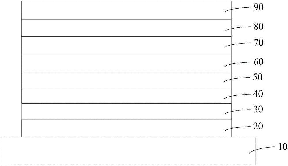
[0048] S221 , providing a substrate 10 and cleaning the substrate 10 .
[0049] The substrate 10 is usually made of glass with high transmittance.
[0050] The operation of cleaning the substrate 10 is as follows: the substrate 10 is ultrasonically treated with detergent, acetone, ethanol and isopropanol for 15 minutes respectively.
[0051] Of course, if the substrate 10 is clean, step S10 can be omitted.
[0052] S222, forming the anode 20 on the substrate.
[0053] The anode 20 is stacked on the surface of the substrate 10 . The anode 20 is a total reflection anode, and the material of the anode 20 is at least one selected from silver,...
Embodiment 1
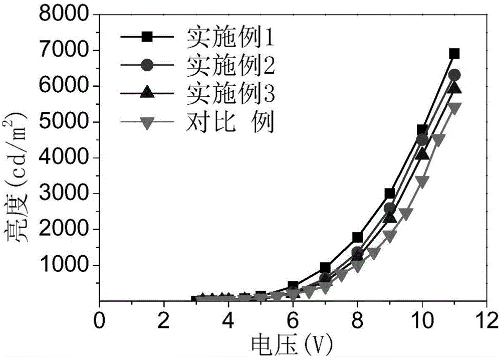
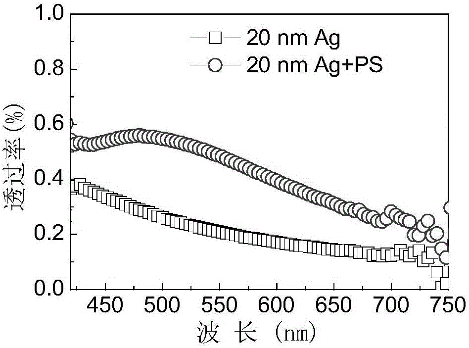
[0094] First, the glass substrate was ultrasonically treated with detergent, acetone, ethanol and isopropanol for 15 min each. On the cleaned glass substrate, Ag with a thickness of 100nm was sequentially evaporated as a reflective anode, and MoO with a thickness of 10nm 3 As hole injection layer, 40nm NPB as hole transport layer, 60nm Alq 3 As the light-emitting layer and electron transport layer, LiF / Al (1nm / 1nm) is used as the electron injection layer, and 20nm Ag is used as the translucent cathode to complete the preparation of top-emitting OLED devices. Then transfer the top-emitting OLED device to an inert atmosphere glove box, and directly spin-coat 35 mg / ml PS solution dissolved in chloroform solution on the translucent cathode Ag of the top-emitting OLED device, rotate at 1500 rpm, and heat at 70°C for 7 minutes to quickly evaporate the solvent , to complete the preparation.
Embodiment 2
[0096] First, the glass substrate was ultrasonically treated with detergent, acetone, ethanol and isopropanol for 15 min each. On the cleaned glass substrate, Ag with a thickness of 100nm was sequentially evaporated as a reflective anode, and MoO with a thickness of 10nm 3 As hole injection layer, 40nm NPB as hole transport layer, 60nm Alq 3 As the light emitting layer and the electron transport layer, LiF / Al (1nm / 1nm) is used as the electron injection layer, and 20nm Ag is used as the translucent cathode to complete the preparation of the top emission OLED device. Then transfer the top-emitting OLED device to an inert atmosphere glove box, and directly spin-coat a 30 mg / ml PS solution dissolved in chloroform solution on the semi-transparent cathode Ag of the top-emitting OLED device, rotate at 1500 rpm, and heat at 70°C for 7 minutes to quickly evaporate the solvent. , to complete the preparation.
PUM
| Property | Measurement | Unit |
|---|---|---|
| Thickness | aaaaa | aaaaa |
| Thickness | aaaaa | aaaaa |
| Thickness | aaaaa | aaaaa |
Abstract
Description
Claims
Application Information
 - Generate Ideas
- Intellectual Property
- Life Sciences
- Materials
- Tech Scout
- Unparalleled Data Quality
- Higher Quality Content
- 60% Fewer Hallucinations
Browse by: Latest US Patents, China's latest patents, Technical Efficacy Thesaurus, Application Domain, Technology Topic, Popular Technical Reports.
© 2025 PatSnap. All rights reserved.Legal|Privacy policy|Modern Slavery Act Transparency Statement|Sitemap|About US| Contact US: help@patsnap.com