Image
Click on the blue label to locate the original text in one second.
Reading with bidirectional positioning of images and text.
Examples
no. 1 Embodiment approach
[0090] Below, refer to Figure 1 to Figure 13 A first embodiment of the liquid crystaldisplay device of the present invention will be described. In addition, in all the following drawings, in order to make drawings easy to see, the thickness of each component, and the ratio of a dimension are made to differ suitably.
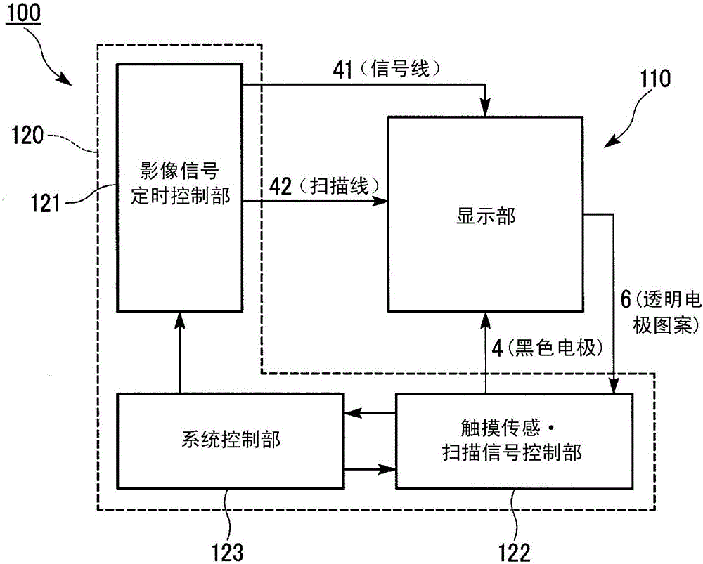
[0091] Such as figure 1 As shown, the liquid crystal display device 100 of this embodiment includes a display unit 110 and a control unit 120 for controlling the display unit 110 and the touch sensing function.
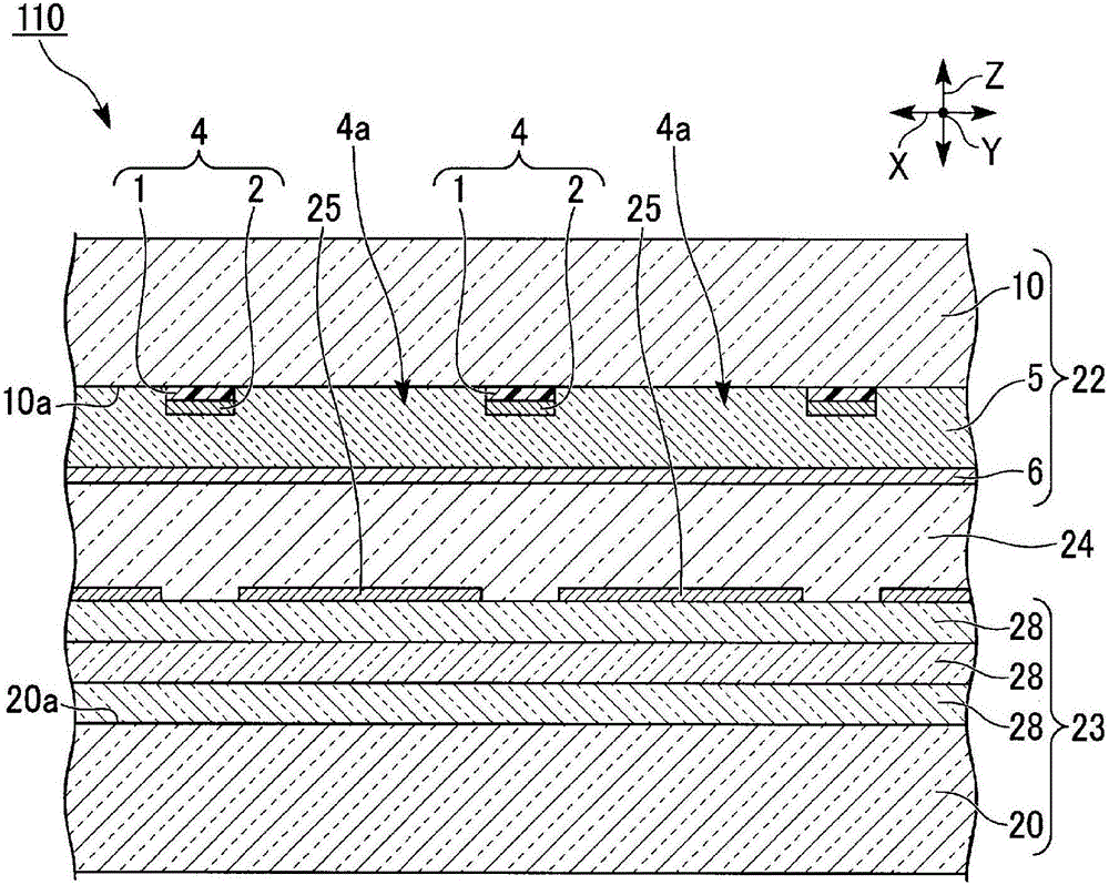
[0092] Such as figure 2 As shown, the display unit 110 has a structure in which a liquid crystal display device substrate (display substrate) 22 , a liquid crystal layer 24 , and an array substrate 23 are laminated in this order. The display unit 110 performs display in a normally black mode. That is, the display unit 110 is formed by bonding a first transparent substrate 10 (described later) of the substrate for liquid crystal display device 22 ...
no. 2 Embodiment approach
[0212] Next, refer to Figure 14 to Figure 17 Although the second embodiment of the present invention will be described, the same reference numerals will be given to the same parts as those in the above-mentioned embodiment to omit the description, and only the different points will be described.
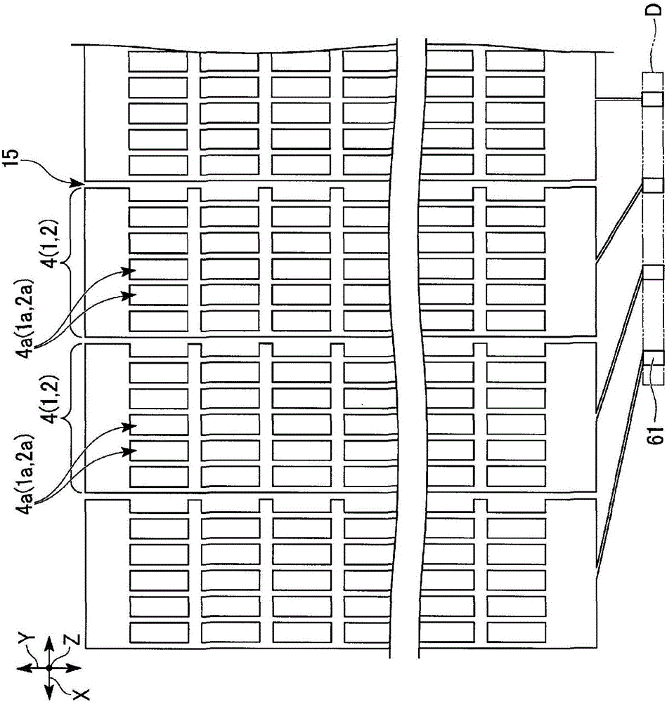
[0213] Such as Figure 14 As shown, the display unit 111 of the present embodiment includes a liquid crystal display device substrate 22A instead of the liquid crystal display device substrate 22 of the display unit 110 of the first embodiment. The substrate 22A for a liquid crystal display device is configured to include a red pixel R formed of a red layer, a green pixel G formed of a green layer, and a pixel opening 4a of the black electrode 4 of the substrate 22 for a liquid crystal display device. Any one of the blue pixels B is formed. These red pixels R, green pixels G, and blue pixels B are inserted between the metal layer pattern 2 and the transparent resin layer 5 along t...
no. 3 Embodiment approach
[0224] Next, a third embodiment of the present invention will be described, but descriptions will be omitted by assigning the same reference numerals to the same parts as in the above-mentioned embodiment, and only different points will be described.
[0225] In this embodiment, except for the configuration of the black electrode 4, that is, the configuration of the metal layer pattern 2, it is the same as the first embodiment. figure 2 . However, overlapping descriptions will be omitted, and the metal layer pattern 2 having a difference will be described. In addition, the black electrode 4 of this embodiment can be used as the black electrode of the said 2nd Embodiment and the 4th Embodiment mentioned later.
[0226] In this embodiment, figure 2 The metal layer pattern 2 shown is a first metal layer (layer) that is a copperalloy containing oxygen with a film thickness of 0.015 μm, and a second metal layer (layer) that is a copper alloy that does not contain oxygen substa...
PUM
Property
Measurement
Unit
reflectivity
aaaaa
aaaaa
coating thickness
aaaaa
aaaaa
reflectivity
aaaaa
aaaaa
Abstract
This LCD device (100) is characterized in that a first transparent substrate (10) on a surface thereof facing a liquid crystal layer (24) is provided with a plurality of light-absorbent resin layer patterns (1), a plurality of metal layer patterns (2), a transparent resin layer (5), and a plurality of transparent electrode patterns (6), laminated in that order; openings are formed in the plurality of light-absorbent resin layer patterns (1) and the plurality of metal layer patterns (2), and are formed to identical shape viewed in the lamination direction; the plurality of metal layer patterns (2) are arranged to line up in a first direction in a mutually insulated state; the plurality of transparent electrode patterns (6) are arranged to line up in a second direction orthogonal to the first direction in a mutually insulated state; the metal layer patterns (2) have at least a copper layer, or an alloy layer in which copper is the principal material; the liquid crystal molecules of the liquid crystal layer (24) have negative dielectric constant anisotropy, and an initial orientation that is a vertical orientation; the display unit produces a normally blank mode display; and the frequency of the touch driving voltage and the liquid crystal driving voltage are different.
Description
technical field [0001] The present invention relates to a liquid crystal display device, which incorporates a touch sensing function into a liquid crystal panel, and has a high aperture ratio and excellent visual recognition. In addition, the present invention can provide a liquid crystal display device including a touch sensing electrode using a low-resistance metal layer pattern suitable for electrodes used in touch sensing and having excellent light-shielding properties for transmitted light. , the reflection color of the metal layer pattern is almost black. In other words, the present invention relates to a so-called in-cellliquid crystal display device in which a capacitive touch sensing function is built in a liquid crystal cell. [0002] This application is based on Japanese Patent Application No. 2014-038821 for which it applied in Japan on February 28, 2014, the priority is claimed, and the content is used for this application. Background technique [0003] In re...
Claims
Application Information
Patent Timeline
Application Date:The date an application was filed.
Publication Date:The date a patent or application was officially published.
First Publication Date:The earliest publication date of a patent with the same application number.
Issue Date:Publication date of the patent grant document.
PCT Entry Date:The Entry date of PCT National Phase.
Estimated Expiry Date:The statutory expiry date of a patent right according to the Patent Law, and it is the longest term of protection that the patent right can achieve without the termination of the patent right due to other reasons(Term extension factor has been taken into account ).
Invalid Date:Actual expiry date is based on effective date or publication date of legal transaction data of invalid patent.

