Pn junction-based logical operation device

A logic operation, pn junction technology, applied in the direction of logic circuits, electrical components, electronic switches with logic functions, etc., can solve the problems of complex structure, high cost, difficult preparation, etc., to achieve low driving voltage and current, simple structure, The effect of broad application prospects

Inactive Publication Date: 2016-11-02
LANZHOU UNIVERSITY
View PDF2 Cites 2 Cited by
  • Summary
  • Abstract
  • Description
  • Claims
  • Application Information

AI Technical Summary

Problems solved by technology

[0002] The development of the information age is inseparable from the promotion of logic circuits. Because logic circuits, especially digital logic circuits, only divide high and low levels, have strong anti-interference ability and high precision, they are widely used in digital communication, automation and other fields, and the composition of logic Most of the basic components of the circuit are bipolar transistors (BJT) and field effect transistors (MOSFET), which are relatively complex in composition, difficult to prepare, and relatively high in cost.

Method used


Image

  • Pn junction-based logical operation device
  • Pn junction-based logical operation device
  • Pn junction-based logical operation device

Examples


Embodiment Construction

[0021] The present invention will be explained in detail below.

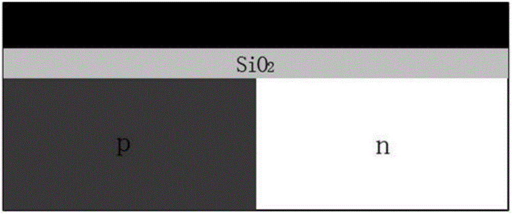
[0022] Inspired by MOSFET, the present invention is innovatively modified on the pn junction of the basic semiconductor device, that is, an insulating dielectric layer is grown on the lateral pn junction, and then an Al electrode is grown. The cross-sectional structure of the device is as attached figure 1 Shown. Since the device is compatible with the traditional pn junction process, it can be made using the traditional pn junction process.

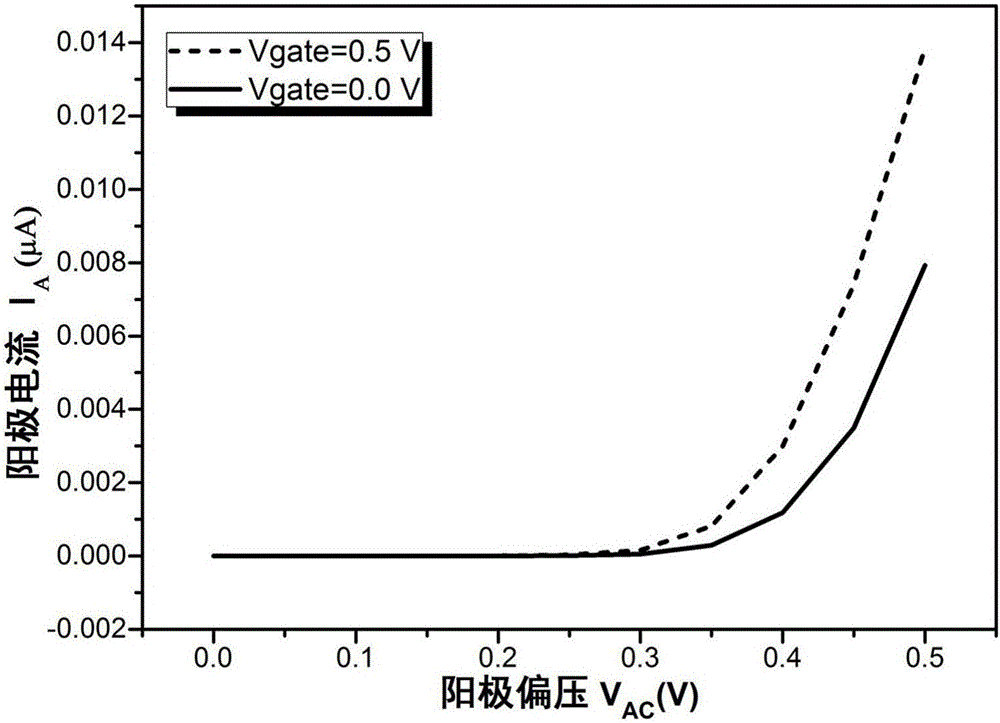
[0023] Because the basic structure of the device is evolved from MOSFET, its working principle is similar to MOSFET. After the gate is biased, an accumulation layer and an inversion layer will be formed in the corresponding place in the channel, thereby changing the conductance of the device channel. Therefore, the I-V characteristics of the device have also changed. The I-V characteristic curve of this component when the gate is applied with high level 0.5V and low level 0V,...


PUM


Abstract

The invention discloses a pn junction-based basic element and a device for realizing the logical circuit operation by using the above element. According to the technical scheme of the pn junction-based element for forming the logical operation device, the logical operation device comprises a pn junction and an electrode formed on an insulating layer outside the pn junction. A grid is composed of the insulating layer arranged on the pn junction and the electrode formed on the insulating layer. A p-type region and an n type region, positioned outside the pn junction, are respectively connected with signal terminals. According to the technical scheme of the invention, the above element can be used for making different logical operation devices. The element is simple in structure and is prepared based on the traditional silicon technology without any other special process. Compared with the traditional BJT and the traditional MOSFET, the device is smaller in size and higher in integration level. Moreover, the device is applicable to a logical operation circuit and can be driven by either voltage or current. Moreover, the device is low in driving voltage and driving current and wide in application prospect.

Description

Technical field [0001] The invention relates to a device that can be used to implement logic circuit operations and a pn junction-based basic element constituting the logic circuit device. Background technique [0002] The development of the information age is inseparable from the promotion of logic circuits. Because logic circuits, especially digital logic circuits, are only divided into high and low levels, have strong anti-interference ability and high accuracy, they are widely used in digital communications, automation and other fields to form logic The basic components of the circuit are mostly bipolar transistors (BJT) and field effect transistors (MOSFET), which are relatively complex in structure, difficult to prepare, and relatively expensive. Summary of the invention [0003] The present invention provides a basic element that can be used to form a logic circuit device, and at the same time provides a logic circuit device composed of such a basic element. [0004] The pn ...

Claims


Application Information

Patent Timeline
Patent Type & Authority Applications(China)
IPC IPC(8): H03K17/56H03K19/20
CPCH03K17/56H03K19/20
Inventor 杨建红杨盼庞正鹏陈健谌文杰
Owner LANZHOU UNIVERSITY
Why Eureka
Try Eureka