A kind of production and processing technology of optical module shell

A processing technology and technology for optical modules, applied in metal processing equipment, manufacturing tools, welding equipment, etc., can solve the problems of coating damage, poor air tightness and firmness, and high production cost of optical module housings, and reduce production and processing costs. Effect

Active Publication Date: 2017-11-21
8TH RES INST OF CETC
View PDF4 Cites 0 Cited by
  • Summary
  • Abstract
  • Description
  • Claims
  • Application Information

AI Technical Summary

Problems solved by technology

[0005] The technical problem to be solved by the present invention is to provide a production and processing process of the optical module housing, which can solve the technical problems of high production cost of the optical module housing, poor airtightness and firmness during packaging, and damage to the coating

Method used


Image

  • A kind of production and processing technology of optical module shell

Examples


Embodiment Construction

[0033] The production and processing technology of an optical module housing of the present invention will be further described in detail in conjunction with specific implementation methods:

[0034] The production and processing technology of a kind of optical module shell of the present invention comprises the following steps:

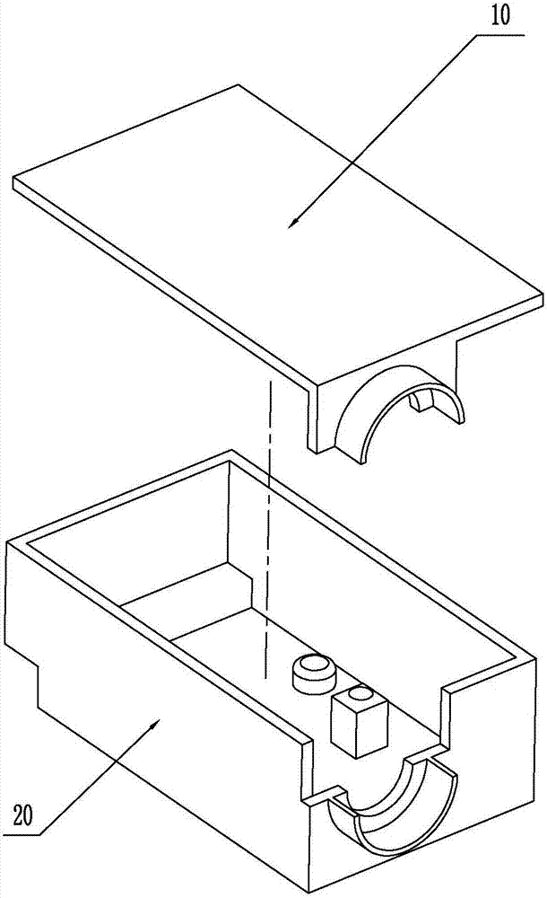
[0035] (1) Zinc alloy material is used to die-cast the optical module housing through die-casting process, see figure 1 , to obtain a cover plate 10 with a thickness of 0.4-0.55 mm and a base 20 with a thickness of 0.6-0.8 mm. The thickness of the cover plate 10 and the base 20 should not be too thin. The most suitable thickness is 0.6-0.8 mm, otherwise the cover plate 10 and the base 20 will be deformed during die-casting, which is not conducive to parallel seam welding, and too thick will increase the cost;

[0036] (2) The surfaces of the cover plate 10 and the base 20 are all nickel-plated, and the thickness of the nickel plating is 18 μm, and o...


PUM

PropertyMeasurementUnit
thicknessaaaaaaaaaa
thicknessaaaaaaaaaa
thicknessaaaaaaaaaa

Abstract

A producing and processing technology for an optical module shell includes the steps that die-cast formation is conducted on the optical module shell through a zinc alloy, and surface nickel plating is conducted, wherein the thickness of a cover plate ranges from 0.4 mm to 0.55 mm, and the thickness of a base ranges from 0.6 mm to 0.8 mm; oxide and impurities on the surface of the cover plate and the surface of the base are removed; the base is placed in a clamp, and the space between the base and the cover plate is coated with soldering flux, wherein the thickness is 0.02 mm; the cover plate is placed on the base without dislocation; the cover plate is pressed downwards with force so that the cover plate, the soldering flux and the base can make close contact; the residual soldering flux is wiped off, and cleanness is kept; it is ensured that the surface of a seam welding electrode is clean and dry; the inner hole wall of the seam welding electrode is coated with conductive grease with the thickness being 0.02 mm, the seam welding electrode is installed on a parallel seam welding machine in the manner that the seam welding electrode can slightly rotate, and the whole seam welding electrode is kept clean; one point is formed at the position of the contact center of cover plate and the base through seam welding, the seam welding electrode is moved to the rightmost end or the leftmost end, and seam welding is started; and a qualified product is obtained. The producing and processing technology solves the problems that the production cost of the optical module shell is high and during packaging, the gas tightness and firmness are poor and a clad layer is damaged.

Description

Technical field: [0001] The invention relates to an optical module housing in an optical communication system, in particular to a production and processing technology for the optical module housing. Background technique: [0002] Optical module housings are widely used in modern optical communication systems and domestic military, aerospace, navigation and other fields. [0003] With the continuous development of information technology, people's requirements for communication technology are getting higher and higher. Optical communication technology has gradually replaced traditional electrical signal communication in various fields, especially in the fields of aerospace, Internet applications, and military information technology. play an irreplaceable role. As an important light source of the optical communication system, the optical module is very necessary to develop its suitable packaging technology. The packaging cost accounts for 50% to 60% of the cost of the optical...

Claims


Application Information

Patent Timeline
Patent Type & Authority Patents(China)
IPC IPC(8): B23P15/00B23K1/20B23K1/14B23K1/00
CPCB23K1/00B23K1/14B23K1/203B23P15/00
Inventor 刘勇周雷吴振刚谢鸿志边敏涛高进刘昭谦杨鹏毅司淑平孙磊
Owner 8TH RES INST OF CETC
Why Eureka
Try Eureka