A semiconductor material containing bismuth and halogen and its preparation and analysis method
A semiconductor and halogen technology, applied in chemical instruments and methods, chemical analysis by titration, bismuth compounds, etc., can solve the problems of materials being unstable to water and not having a perovskite-like structure, and achieve stable and reliable product properties The effect of mild control and reaction conditions
- Summary
- Abstract
- Description
- Claims
- Application Information
AI Technical Summary
Problems solved by technology
Method used
Image
Examples
Embodiment 1
[0043] Example 1: Cs 3 Bi 2 Br 3 I 6
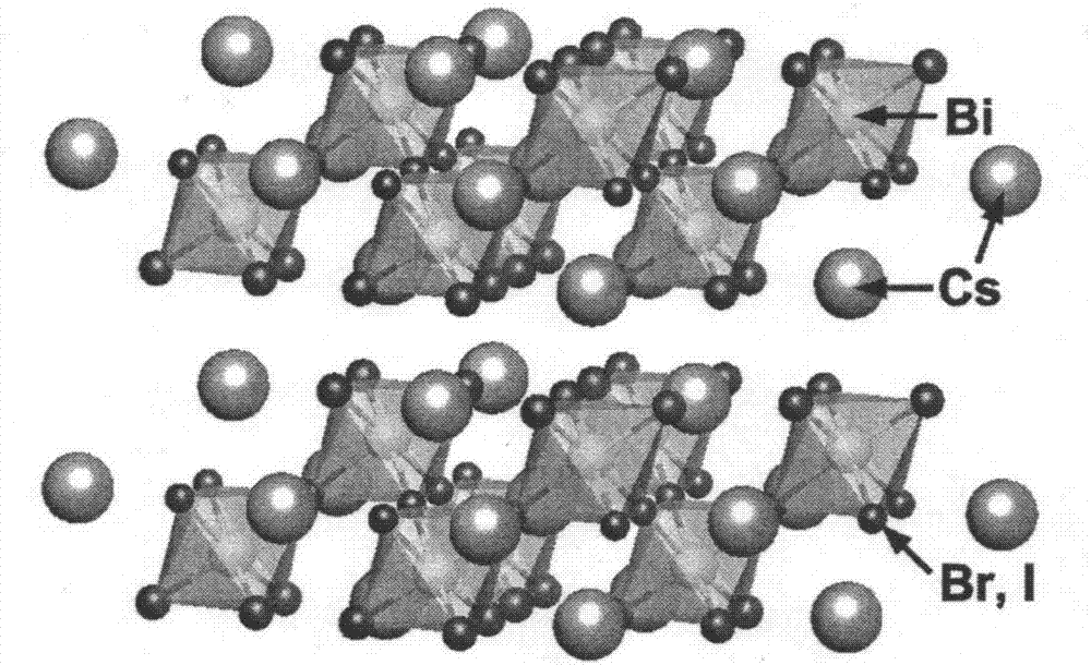
[0044] A semiconducting material containing bismuth and halogens with the chemical formula Cs 3 Bi 2 Br 3 I 6 , has a perovskite-like crystal structure, the space group is P-3m1, and its preparation method is:
[0045]
[0046] Accurately weigh 588mg (0.300mmol) of Cs 3 Bi 2 I 9 With 230mg (0.150mmol) of Cs 3 Bi 2 Br 9 Grind and mix evenly and put it into a glass ampoule, evacuate to below 20Pa, fill it with 1 / 3 atmospheric pressure of nitrogen and seal it, and heat to 640°C under the protection of nitrogen to react for 6 hours to obtain a red-black solid.
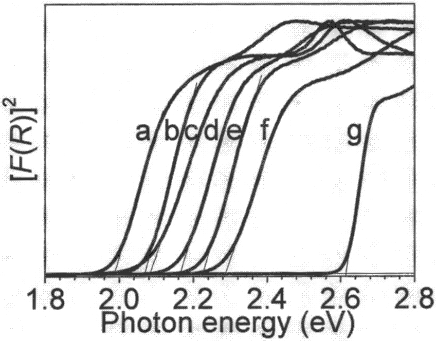
[0047] Visible diffuse reflectance spectrum as figure 2 As shown in curve b, the optical bandgap E g =2.07eV.
[0048] The powder XRD pattern is as follows Figure 5 As shown, the result of unit cell refinement: Trigonal crystal system, P-3m1 space group (No.164), lattice parameters Molecular formula volume The unit cell refinement results show that the semico...
Embodiment 2
[0055] Example 2: Cs 3 Bi 2 BrI 8
[0056] A semiconducting material containing bismuth and halogens with the chemical formula Cs 3 Bi 2 BrI 8 , has a perovskite-like crystal structure, the space group is P-3m1, and its preparation method is:
[0057]
[0058] Accurately weigh 784mg (0.400mmol) of Cs 3 Bi 2 I 9 With 76.8mg (0.0500mmol) of Cs 3 Bi 2 Br 9 Grind and mix evenly and put it into a glass ampoule, evacuate to below 20Pa, fill with 1 / 3 atmospheric pressure of nitrogen and seal it, heat to 550°C under nitrogen protection and react for 6 hours to obtain a red-black solid.
[0059] Visible diffuse reflectance spectrum as figure 2 As shown in curve a, the optical bandgap E g = 1.99eV.
[0060] The powder XRD pattern is as follows Figure 6 As shown, the result of unit cell refinement: Trigonal crystal system, P-3m1 space group (No.164), lattice parameters Molecular formula volume The unit cell refinement results show that the semiconductor material co...
Embodiment 3
[0067] Example 3: Cs 3 Bi 2 Br 6 I 3
[0068] A semiconducting material containing bismuth and halogens with the chemical formula Cs 3 Bi 2 Br 6 I 3 , has a perovskite-like crystal structure, the space group is P-3m1, and its preparation method is:
[0069]
[0070] Accurately weigh 294mg (0.150mmol) of Cs 3 Bi 2 I 9 with 461mg (0.300mmol) of Cs 3 Bi 2 Br 9 Grind and mix evenly and put it into a glass ampoule, evacuate to below 20Pa, fill it with 1 / 3 atmospheric pressure of nitrogen, seal it, and heat it to 640°C for 6 hours to obtain an orange-red solid.
[0071] Visible diffuse reflectance spectrum as figure 2 As shown in curve e, the optical bandgap E g = 2.23eV.
[0072] The powder XRD pattern is as follows Figure 7 As shown, the result of unit cell refinement: Trigonal crystal system, P-3m1 space group (No.164), lattice parameters Molecular formula volume The unit cell refinement results show that the semiconductor material containing bismuth and...
PUM
| Property | Measurement | Unit |
|---|---|---|
| optical band gap | aaaaa | aaaaa |
| optical band gap | aaaaa | aaaaa |
| optical band gap | aaaaa | aaaaa |
Abstract
Description
Claims
Application Information


