

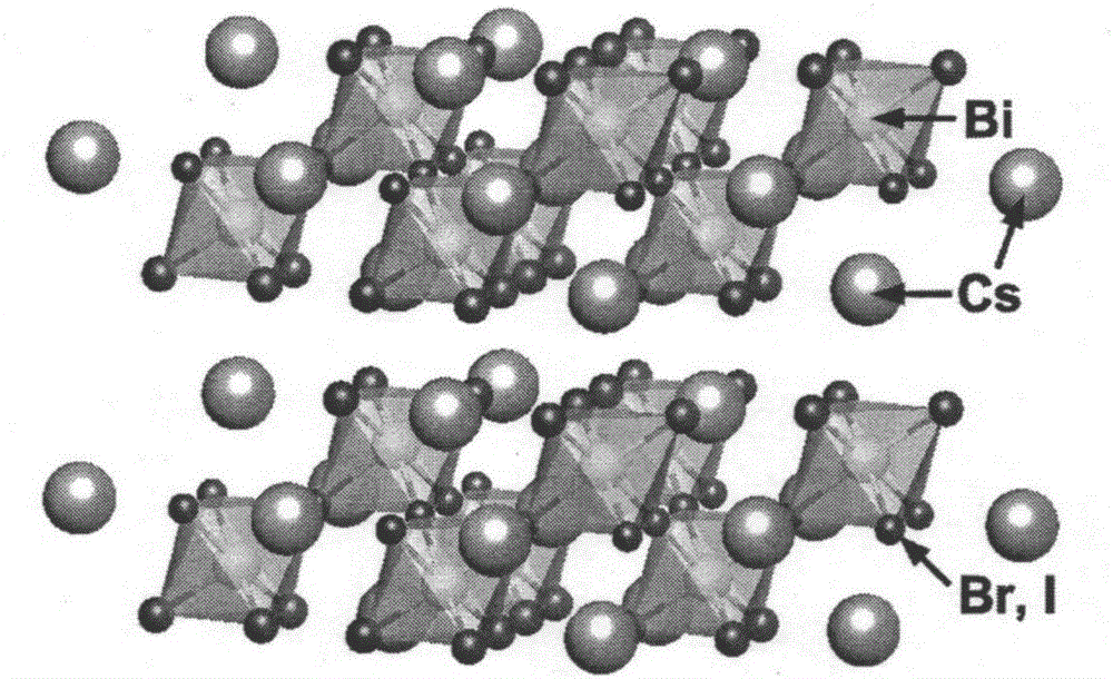
Semiconductor material containing bismuth and halogen and preparation and analysis method thereof
An analytical method and semiconductor technology, applied in chemical instruments and methods, chemical analysis by titration, bismuth compounds, etc., can solve the problems of not having a perovskite-like structure, the material is unstable to water, etc., and achieve stable product properties. Controlled, mild reaction conditions
- Summary
- Abstract
- Description
- Claims
- Application Information
AI Technical Summary
Problems solved by technology
Method used
Image

Examples
Embodiment 1
[0043] Example 1: Cs 3 Bi 2 Br 3 I 6
[0044] A semiconducting material containing bismuth and halogens with the chemical formula Cs 3 Bi 2 Br 3 I 6 , has a perovskite-like crystal structure, the space group is P-3m1, and its preparation method is:
[0045]
[0046] Accurately weigh 588mg (0.300mmol) of Cs 3 Bi 2 I 9 With 230mg (0.150mmol) of Cs 3 Bi 2 Br 9 Grind and mix evenly and put it into a glass ampoule, evacuate to below 20Pa, fill it with 1 / 3 atmospheric pressure of nitrogen and seal it, and heat to 640°C under the protection of nitrogen to react for 6 hours to obtain a red-black solid.
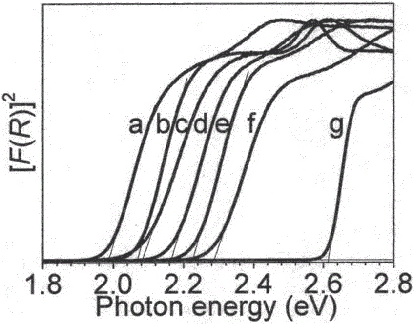
[0047] Visible diffuse reflectance spectrum as figure 2 As shown in curve b, the optical bandgap E g =2.07eV.
[0048] The powder XRD pattern is as follows Figure 5 As shown, the result of unit cell refinement: Trigonal crystal system, P-3m1 space group (No.164), lattice parameters Molecular formula volume The unit cell refinement results show that the semico...
Embodiment 2
[0055] Example 2: Cs 3 Bi 2 BrI 8
[0056] A semiconducting material containing bismuth and halogens with the chemical formula Cs 3 Bi 2 BrI 8 , has a perovskite-like crystal structure, the space group is P-3m1, and its preparation method is:
[0057]
[0058] Accurately weigh 784mg (0.400mmol) of Cs 3 Bi 2 I 9 With 76.8mg (0.0500mmol) of Cs 3 Bi 2 Br 9 Grind and mix evenly and put it into a glass ampoule, evacuate to below 20Pa, fill with 1 / 3 atmospheric pressure of nitrogen and seal it, heat to 550°C under nitrogen protection and react for 6 hours to obtain a red-black solid.
[0059] Visible diffuse reflectance spectrum as figure 2 As shown in curve a, the optical bandgap E g = 1.99eV.
[0060] The powder XRD pattern is as follows Figure 6 As shown, the result of unit cell refinement: Trigonal crystal system, P-3m1 space group (No.164), lattice parameters Molecular formula volume The unit cell refinement results show that the semiconductor material co...
Embodiment 3
[0067] Example 3: Cs 3 Bi 2 Br 6 I 3
[0068] A semiconducting material containing bismuth and halogens with the chemical formula Cs 3 Bi 2 Br 6 I 3 , has a perovskite-like crystal structure, the space group is P-3m1, and its preparation method is:
[0069]
[0070] Accurately weigh 294mg (0.150mmol) of Cs 3 Bi 2 I 9 with 461mg (0.300mmol) of Cs 3 Bi 2 Br 9 Grind and mix evenly and put it into a glass ampoule, evacuate to below 20Pa, fill it with 1 / 3 atmospheric pressure of nitrogen, seal it, and heat it to 640°C for 6 hours to obtain an orange-red solid.
[0071] Visible diffuse reflectance spectrum as figure 2 As shown in curve e, the optical bandgap E g = 2.23eV.
[0072] The powder XRD pattern is as follows Figure 7 As shown, the result of unit cell refinement: Trigonal crystal system, P-3m1 space group (No.164), lattice parameters Molecular formula volume The unit cell refinement results show that the semiconductor material containing bismuth and...
PUM
| Property | Measurement | Unit |
|---|---|---|
| optical band gap | aaaaa | aaaaa |
| optical band gap | aaaaa | aaaaa |
| optical band gap | aaaaa | aaaaa |
Abstract
Description
Claims
Application Information