Backside illuminated global exposure pixel unit structure and manufacturing method

A technology of pixel unit and global exposure, applied in the field of image sensors, can solve the problems of inability to effectively reduce the readout noise of the pixel unit, reduce the photodiode photosensitive area, reduce the sensitivity of the pixel unit, etc., so as to reduce the readout noise and prevent distortion. , avoid the effect of influence

Active Publication Date: 2016-11-09
SHANGHAI INTEGRATED CIRCUIT RES & DEV CENT +1
View PDF3 Cites 8 Cited by
  • Summary
  • Abstract
  • Description
  • Claims
  • Application Information

AI Technical Summary

Problems solved by technology

[0015] At the same time, those skilled in the art know that the capacitance values ​​of the storage capacitor C1 and the storage capacitor C2 also directly affect the readout noise of the global exposure pixel unit, the larger the capacitance value of the storage capacitor C1 and the storage capacitor C2, the higher the readout noise of the pixel unit The smaller the size, the better the performance. Conventional storage capacitors C1 and C2 use MOS storage capacitors. The capacitance value is proportional to its area. However, if the area of ​​the storage capacitor is increased, the photosensitive area of ​​the photodiode needs to be reduced. Will reduce the sensitivity of the pixel unit
like figure 2 As shown, the lower plate of the MOS capacitor is located in the silicon substrate. In order to ensure the sensitivity of the pixel unit, we hope to increase the photosensitive area, that is, the area of ​​the photodiode as much as possible. However, the area of ​​the front-illuminated MOS capacitor is limited by the photodiode, namely The capacitance value of the MOS capacitor is limited, that is, the readout noise of the pixel unit cannot be effectively reduced
[0016] Therefore, in order to ensure the photosensitive area of ​​the photodiode region in the pixel unit, the area of ​​the storage capacitor is limited

Method used


Image

  • Backside illuminated global exposure pixel unit structure and manufacturing method
  • Backside illuminated global exposure pixel unit structure and manufacturing method
  • Backside illuminated global exposure pixel unit structure and manufacturing method

Examples


Embodiment Construction

[0041] In order to make the content of the present invention clearer and easier to understand, the content of the present invention will be further described below in conjunction with the accompanying drawings. Of course, the present invention is not limited to this specific embodiment, and general replacements known to those skilled in the art are also covered within the protection scope of the present invention. Secondly, the present invention is described in detail by means of schematic diagrams. When describing the examples of the present invention in detail, for the convenience of explanation, the schematic diagrams are not partially enlarged according to the general scale, which should not be used as a limitation of the present invention.

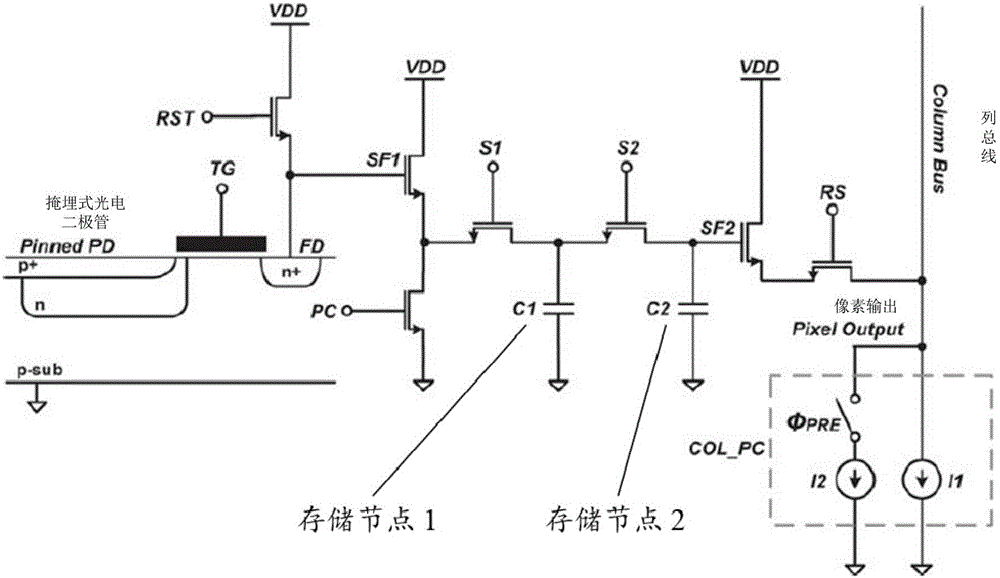
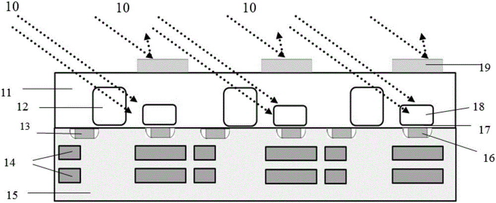
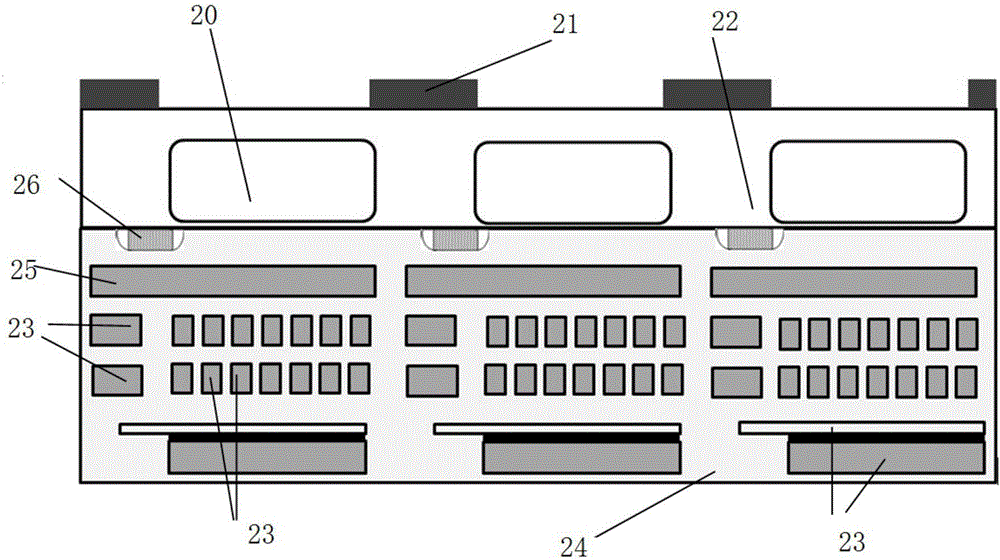
[0042] see image 3 , image 3 It is the structural intention of the back-illuminated global exposure pixel unit of the present invention. As shown in the figure, in the embodiment of the present invention, the pixel unit structure ...


PUM


Abstract

The invention relates to a backside illuminated global exposure pixel unit structure and a manufacturing method. The pixel unit structure comprises a substrate at the upper part and a dielectric structure located at the lower part, wherein a plurality of photodiodes are formed in the substrate; a pass transistor grid polycrystalline layer, a light blocking block layer and a storage capacitor are sequentially formed in the dielectric structure from top to bottom; and the light blocking block layer is used for blocking light which penetrates through the photodiodes. Therefore, the influence of incident light on a charge signal in the signal storage capacitor can be avoided; the capacitance of the storage capacitor is increased; readout noise is reduced; the area of the photodiodes for photoreception in the pixel unit can also be increased; the sensitivity of the global exposure pixel unit is improved; and a high-quality image can be finally obtained by an image sensor.

Description

technical field [0001] The invention relates to the field of image sensors, in particular to a structure of a back-illuminated global exposure pixel unit and a manufacturing method thereof. Background technique [0002] An image sensor refers to a device that converts an optical signal into an electrical signal. Usually, a large-scale commercial image sensor chip includes a charge-coupled device (Charge-coupled Device referred to as CCD) and a complementary metal oxide semiconductor (Complementary Metal Oxide Semiconductor referred to as CMOS) image sensor. There are two types of chips. [0003] Compared with traditional CCD sensors, CMOS image sensors have the characteristics of low power consumption, low cost and compatibility with CMOS technology, so they are more and more widely used. CMOS image sensors are now not only used in consumer electronics such as miniature digital cameras (DSC), mobile phone cameras, video cameras, and digital single-lens reflex (DSLR), but al...

Claims


Application Information

Patent Timeline
Patent Type & Authority Applications(China)
IPC IPC(8): H01L27/146
CPCH01L27/14643H01L27/14683
Inventor 顾学强赵宇航周伟
Owner SHANGHAI INTEGRATED CIRCUIT RES & DEV CENT
Why Eureka
Try Eureka